Solder paste inspection with 3D imaging
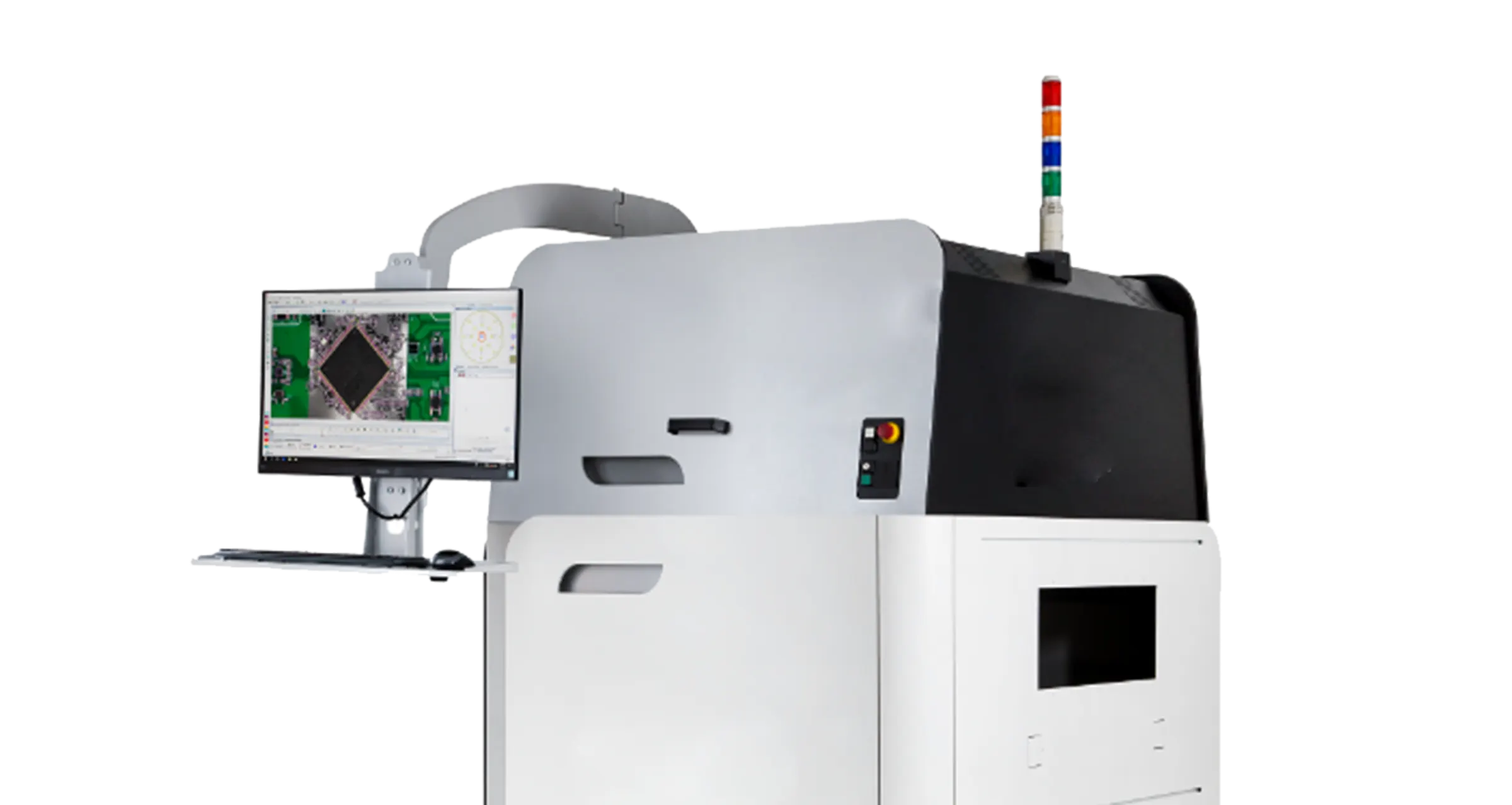
Solder paste inspection occurs during the production of electronic components, ensuring that the paste was correctly applied. 3D imaging is used to measure the alignment and volume of the solder paste, allowing for early detection of any defects. This enables immediate corrective action to take place before components are permanently connected.

Printing the solder paste:
a critical manufacturing step
More than 50% of PCB manufacturing defects are due to improper solder paste printing. If paste printing is not done correctly, the error can affect subsequent assembly and soldering processes, resulting in a skewed component or a poor, defective, or even missing solder joint. Inspecting the solder paste is therefore critical to PCB manufacturing.

Solder paste measurements
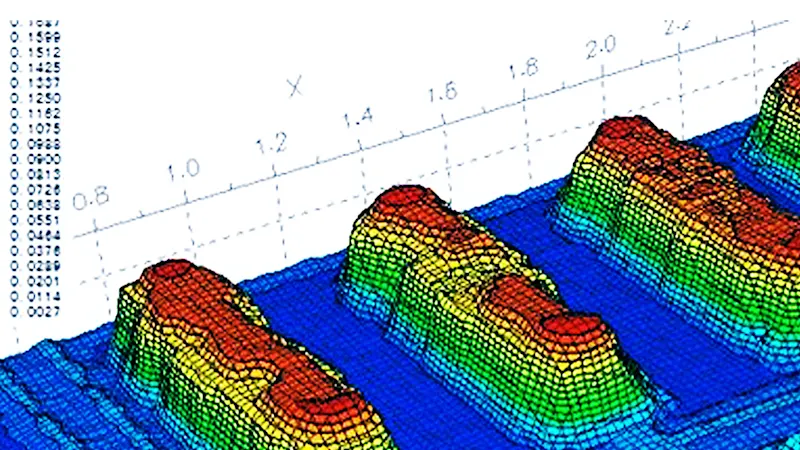
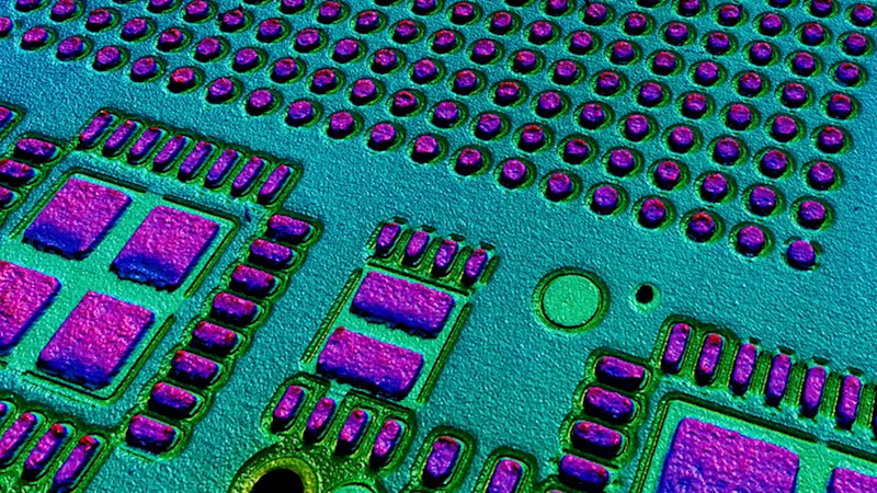
3D camera systems are able to measure the surface, height, profile, and volume of the solder paste. This allows defects such as offset paste, insufficient paste, excess paste, or paste smearing to be made apparent. Defects in the application of the solder wicking or bridging also become evident.

AI-based image comparison
Imaging systems with AI can identify defects in solder paste by comparing images. The neural network is trained with images of PCBs with correctly applied solder and those with solder defects. With high reliability, the system captures images during the manufacturing process, compares them with previous PCB images stored in the system, and evaluates the quality.
pylon AI enables complex image analyses for precise verification of the solder paste application. Use your own data sets, flexibly choose from ONNX AI models, and optimize your AI model for your target processing hardware. pylon AI can be used quickly and easily without any programming.
Choose the right resolution and speed
Selecting the appropriate resolution is one of the most important parameters in the visual inspection of solder paste printing. The resolution usually depends on the required inspection speed and accuracy.
The resolution of the camera sensor determines the field of view (FOV). Larger fields of view mean that the PCB can be scanned with fewer images, however: cameras with a higher pixel count require more time to capture each image. Cameras with lower pixel counts have a smaller field of view, but require much less time to capture a new image. The resulting higher frame rate can be used to cover a large PCB area with dynamic imaging without interrupting the acquisition of each image.
Our solution

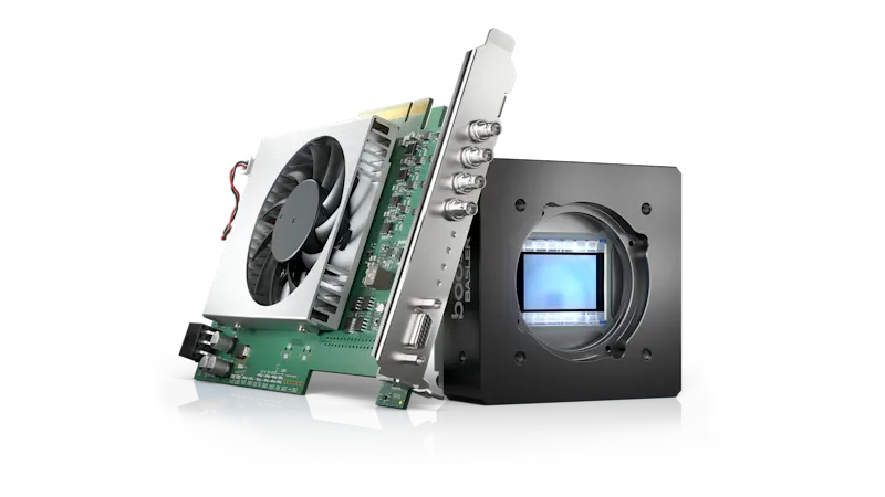
Imaging system including a matching camera and acquisition card give a clear view
The boost area scan camera provides an optimal balance of high resolution and high frame rate. Models with 1:1 aspect ratio offer higher FOV accuracy.
C-mount lenses as a cost-effective lens standard
Compatible interface cards are integration-ready
Large selection of matching accessories for a stable overall system with optimum price/performance ratio
Complete 3D SPI machines and manufacturing systems typically handle the aforementioned steps. If you are interested in this option, we are happy to support you with your application and the design-in process of your system.
Learn more about our project-specific services