What Really Limits Microscopy Resolution?
Diffraction, Rayleigh, aberrations, and Nyquist sampling explained
Explore the theoretical and practical limits of microscopy resolution, equipping vision engineers with the essential insight needed to assess optical constraints and define high-resolution imaging system requirements.
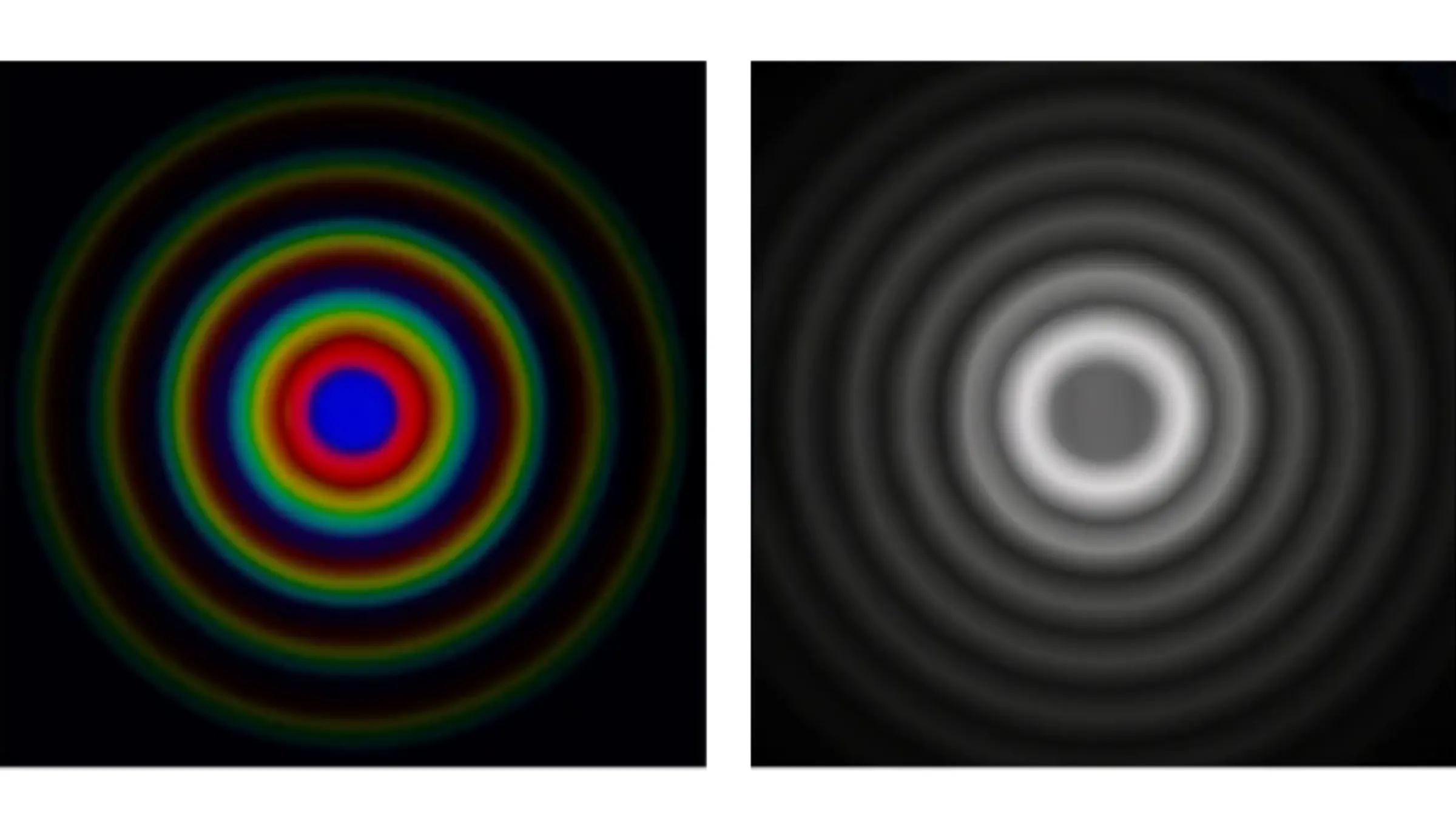
For better understanding
For a clear introduction to magnification, numerical aperture (NA), and their impact on resolution and image quality, read the foundational article Magnification, Numerical Aperture (NA), and Resolution in Microscopic Imaging before you get started.
To the Article: Magnification, NA & Resolution1. Understanding microscopy resolution
Optical microscopy resolution refers to the ability of an imaging system to clearly distinguish fine details within a specimen. In high-precision applications such as semiconductor inspection, it is a critical parameter that directly impacts system performance. However, no matter how many megapixels a camera sensor offers, the smallest feature it can resolve is ultimately limited by fundamental optical principles.
To understand, and potentially overcome these limits, we need to look at four interrelated core concepts: Abbe Diffraction Limit, Rayleigh Criterion, Optical Aberrations, and Nyquist Sampling.
2. Diffraction: the fundamental physical limit
Abbe diffraction limit
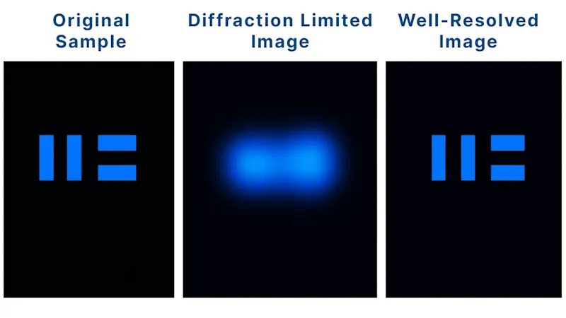
The Abbe diffraction limit describes the fundamental physical barrier to optical resolution, arising from light’s wave nature. Diffraction is an unavoidable physical limit. In 1873, Ernst Abbe formulated a quantitative description of this limit, expressed as: d = λ /(2*NA)
where:
d is the smallest resolvable feature size (resolution)
λ is the illumination wavelength
According to this equation, using shorter wavelengths and optics with higher numerical aperture (NA) improves resolution. NA depends on both the refractive index of the imaging medium and the maximum light collection angle.
For example, using 500 nm illumination with a 1.4 NA oil immersion objective yields an ideal limit near 179 nm. However, practical constraints such as polychromatic illumination and lens design typically result in ~200 nm being the achievable lateral resolution in real systems.
Rayleigh criterion
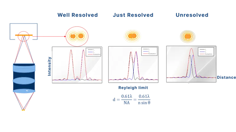
While Abbe’s formula gives the theoretical lower bound of resolution, practical systems also need a criterion to determine when two points are just “distinguishable.” The Rayleigh criterion defines this by stating that two point sources are resolvable when the central peak of one Airy disk coincides with the first dark ring of another: d=0.61λ / NA
Rayleigh’s criterion is particularly useful for assessing the visibility of isolated features under partially coherent or incoherent illumination, such as particle detection or contamination analysis. It's common to see specifications like “Resolution (Rayleigh): 0.85 µm at 550 nm” in industrial optics datasheets, ensuring enough contrast for reliable automated inspection.
While Abbe’s formula sets the theoretical resolution limit by defining the finest spatial detail an optical system can transmit, the Rayleigh criterion provides a practical threshold for when two features can be reliably distinguished in real images. These two ideas are complementary: Abbe guides choices like illumination wavelength and objective NA to set the system’s fundamental limits, while Rayleigh ensures that those limits translate into usable contrast and separability in practice. Both must be considered together when designing optical systems that balance resolution and image quality.
3. Aberrations: the real-world practical limit
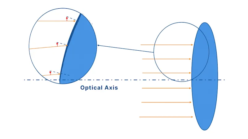
Even systems designed to meet the Abbe limit or Rayleigh criterion in theory face a critical real-world challenge: optical aberrations.
Optical aberrations are deviations from perfect focusing that blur images, distort them, or broaden the point spread function (PSF), reducing effective resolution. A system designed for 200 nm resolution might deliver 300 nm or worse with poorly controlled aberrations.
These aberrations arise because, although Snell's Law describes how rays refract at surfaces, it does not ensure that all the rays from an object converge perfectly to a single image point. Designing lenses that satisfy Snell's Law while achieving perfect imaging for all rays is extremely challenging, and real lenses inevitably have imperfections—shape variations, material inhomogeneities, and assembly tolerances—that create wavefront distortions preventing precise convergence.
Optical aberrations represent an unavoidable practical limit, though careful engineering can minimize their impact.
The aperture-aberration tradeoff
Larger apertures theoretically improve resolution but worsen aberrations in practice, creating a fundamental design compromise.
The diagrams below show that wider apertures allow more light through but cause peripheral rays to experience greater aberrations at extreme angles. Using only the lens center reduces aberrations but limits light-gathering power.
Solutions: Find the optimal numerical aperture balancing resolution against aberrations, or use aspherical lenses and multi-element lens combinations to compensate for aberrations while maintaining larger apertures.


4. Nyquist Sampling Criterion: the final detection limit
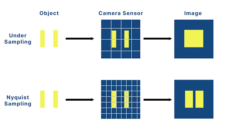
While diffraction and aberrations set the optical limits of resolution, the final image quality also depends on whether the sensor can accurately capture that detail. This is where the Nyquist sampling criterion becomes essential.
In imaging, this criterion states that to accurately reconstruct spatial detail, the sampling frequency must be at least twice the desired resolution. The Nyquist theorem requires:
Effective Sampling pitch ≤ Optical resolution/2
In other words:
Effective Sampling pitch = Camera pixel size/Magnification ≤ d/2
When optical images form on sensors, continuous light distributions are sampled by discrete pixel arrays. If pixels are too large (undersampling), the system cannot resolve fine details, causing aliasing—where high-frequency structures appear as lower-frequency artifacts. This creates blurred images, jagged edges, and false moiré patterns.
Practical design considers a safety factor
While Nyquist theoretically requires exactly 2× sampling, real-world design needs extra margin for edge effects, aberrations, noise, imperfect optical MTF, and varying illumination conditions. Vision engineers typically add an empirical safety factor K of around 1.1–1.3, modifying the formula to:
Camera Pixel Size/Magnification ≤ d/(2K)
Using the midpoint value of K = 1.15 results in the commonly used industry multiplier of 2.3.
5. From formula to design: detecting 2 μm defects
Now let's apply these formulas to a concrete microscopy example: designing a system to detect 2 μm defects reliably. The following steps show how these resolution limits work together in real-world design decisions.
Steps | Tasks | Actions and Results |
|---|---|---|
1 | Calculate Required Optical Resolution | Use Rayleigh criterion: d = 0.61λ/NA with 550 nm green light. For 2 μm resolution: NA ≥ 0.17. Choose NA = 0.3 for design margin, giving theoretical resolution ≈ 1.1 μm. |
2 | Choose or Design the Optics | Select an objective lens with NA ≥ 0.3. Minimize aberrations using aspherical elements or multi-element designs for diffraction-limited performance. |
3 | Calculate Sampling Requirements | Apply Nyquist criterion with safety factor (K = 1.15) Effective pixel size ≤ 2 μm / (2 × 1.15) ≈ 0.87 μm. |
4 | Choose Camera and Magnification | To achieve ≤ 0.87 μm sampling pitch: Note: smaller pixels allow lower magnification and larger field of view. |
Required pixel size to match microscope optical resolution
Objective (Numerical Aperture) | Resolution Limit (µm) | Projected Size (µm) | Required Pixel Size (µm) |
1× (0.04) | 6.9 | 6.9 | 3.5 |
|---|---|---|---|
2× (0.06) | 4.6 | 9.2 | 4.6 |
2× (0.10) | 2.8 | 5.6 | 2.8 |
4× (0.10) | 2.8 | 11.2 | 5.6 |
4× (0.12) | 2.3 | 9.2 | 4.6 |
4× (0.20) | 1.4 | 5.6 | 2.8 |
10× (0.25) | 1.1 | 11.0 | 5.5 |
10× (0.30) | 0.92 | 9.2 | 4.6 |
10× (0.45) | 0.61 | 6.1 | 3.0 |
20× (0.40) | 0.69 | 13.8 | 6.9 |
20× (0.50) | 0.55 | 11.0 | 5.5 |
20× (0.75) | 0.37 | 7.4 | 3.7 |
6. Industrial implementation: semiconductor inspection

In semiconductor inspection, high-resolution microscopy is essential for detecting sub-micron defects, verifying critical dimensions, and ensuring precise overlay alignment. Each of the limits discussed in this article—diffraction, the Rayleigh criterion, optical aberrations, and Nyquist sampling—plays a direct role in shaping the design of optical inspection systems for semiconductor manufacturing.
The diffraction and Rayleigh limits define the theoretical minimum feature size that optics can resolve, setting requirements for illumination wavelength and numerical aperture (NA). Aberrations introduce real-world deviations that degrade resolution and measurement accuracy if not carefully managed, necessitating advanced lens designs and precise alignment. Nyquist sampling ensures that, once optical resolution is achieved, the camera’s pixel size and system magnification correctly capture fine details on the wafer without aliasing.

But these principles alone don’t guarantee success on the production line. Other critical factors—such as the system’s Modulation Transfer Function (MTF), illumination coherence, depth of field, signal-to-noise ratio (SNR), sample surface properties, and environmental stability—all impact final imaging performance. For semiconductor inspection tasks like large-area wafer scanning or overlay metrology, consistent, sub-micron accuracy requires rigorous system-level engineering.
Moving from theoretical design to lab prototype to factory-floor deployment involves balancing these trade-offs, performing extensive testing, and refining the setup for real production conditions. That’s why building reliable semiconductor inspection systems is not just about knowing optical theory—but also working with experienced vision engineers who can integrate all these factors into a robust, production-ready solution.
For project-specific optical questions? Consult our experienced engineer.