Macro Surface Defect Inspection with Full Wafer Imaging
Advancing Semiconductor Vision Inspection
Increased demand, advancing complexity: semiconductor inspection is expanding in precision and capacity to meet the needs of fabrication capabilities. As silicon wafers and glass panels grow in scale, increasing resolution, speed, and reliability of the vision system is a necessity.
Last updated: 03/01/2026
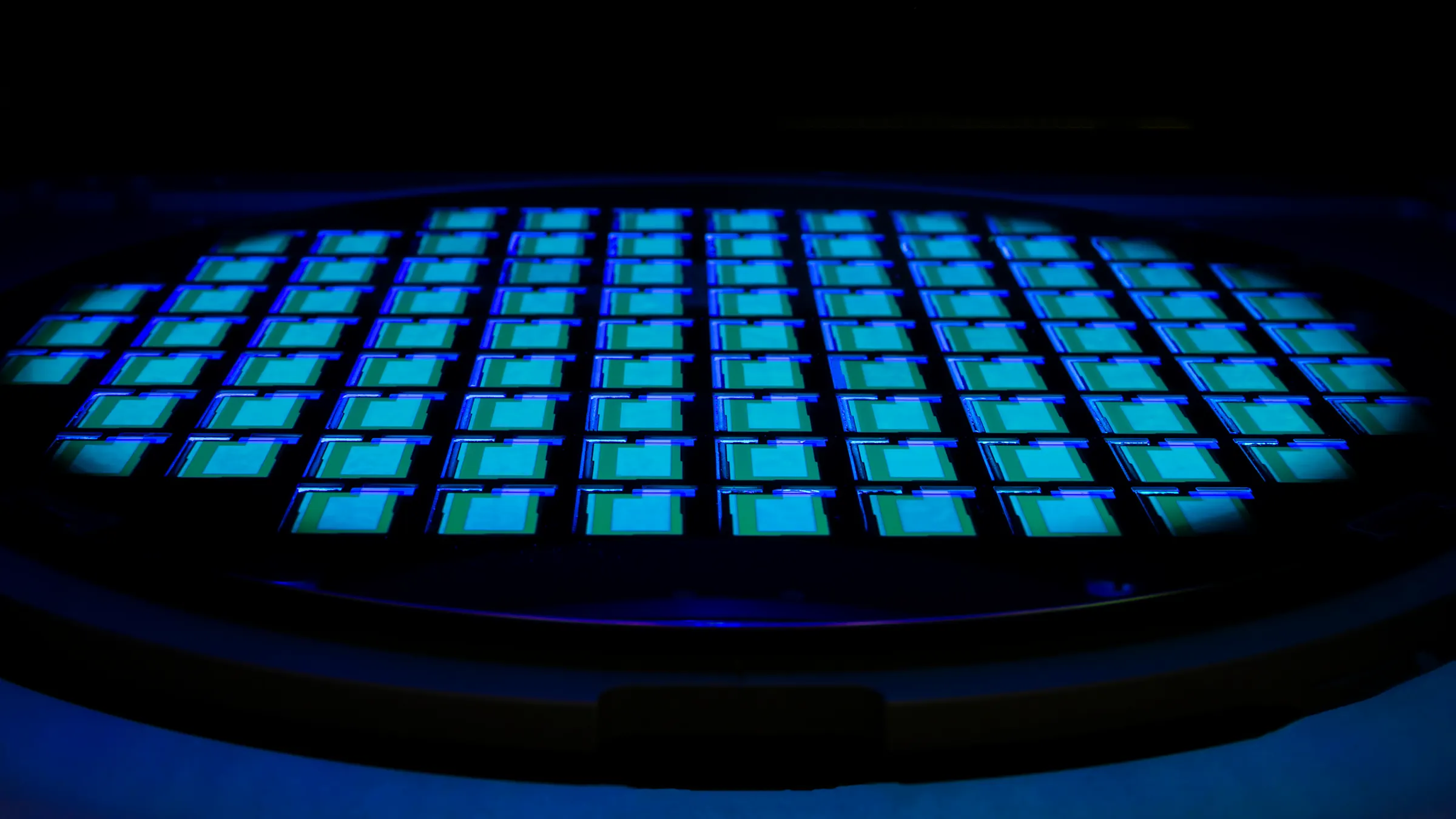
Macro surface defect inspection with full-wafer imaging
Macro surface defect inspection is the primary and most critical application of full-wafer imaging in semiconductor manufacturing. Macro surface defects are large-scale surface anomalies that can occur during front-end semiconductor processes.
As semiconductor devices continue to scale to smaller nodes and support fast-growing markets such as artificial intelligence (AI), electric vehicles (EVs) and advanced automotive systems, defect tolerance continues to shrink. In high-reliability applications, including ADAS, autonomous driving, and aerospace, chip failure is not an option. Comprehensive macro surface defect inspection is therefore a foundational requirement for modern semiconductor manufacturing.
What are macro surface defects?
Macro surface defects are visible, wafer-level imperfections that can negatively impact device performance, yield and reliability. Common examples include:
Large particles and contamination
Scratches and surface damage
Haze, stains or discoloration
Pattern irregularities and non-uniformities
When does macro surface defect inspection occur?
Macro surface defect inspection is typically performed after key front-end-of-line (FEOL) processes, including:
Post-lithography
Post-etch
Post-CMP
Why macro surface defect inspection is critical
Detecting macro surface defects early is essential to maintaining high yield and preventing downstream failures. In addition to reducing scrap and rework, macro defect inspection helps protect manufacturing tools and equipment. Certain defects can cause mechanical or process-related incidents inside tools, leading to unplanned downtime and costly repairs.
Because macro surface defects are not localized and can appear anywhere across the substrate, inspecting only selected regions is insufficient. Full-wafer imaging captures the entire wafer or panel in a single, consistent dataset, enabling reliable detection of large-area defects and supporting repeatable, high-throughput inspection workflows.
Full-Wafer Imaging at High Resolution and Inspection Speed
Full wafer imaging captures high-resolution images of the entire surface of a silicon wafer. It is critical for quality control, process monitoring, and yield analysis. Full wafer imaging can either be done in a single shot or through rapid scanning.
Full wafer imaging can support wafer production in different ways:
Performs wafer positioning and alignment, including notch finding and active wafer centering.
Performs code reading for end-to-end traceability.
Verifies print quality and structural integrity.
Streamlines inspection workflows and reduces manual steps.
Supports scalability as sizes and tool complexity increase.
Achieving high demands may require customizing components to meet exact performance targets within system constraints.
Let's talk about your projectTailored solutions for 300 mm full wafer imaging
Full wafer & glass substrate imaging of 300 mm wafers presents a particular challenge, driven by the scale, precision, and throughput requirements of the modern fab. There is an inherent balance between surface-macro defect sensitivity and overall system throughput, as increases in pixel density can drive higher processing loads.
To address this, there are three core approaches to maintaining image resolution while enlarging the field of view, ensuring consistent performance, speed, and sensitivity across 300 mm and beyond.

Snapshot with large resolution
Benefits:
Captures a single shot with a large field of view and resolution that measures macro defects of one hundred micrometers or larger.
Prevents motion artifacts through the global shutter.
Performs fast on framegrabber processing for flat field correction and distortion correction.

Multicamera + Stitching
Benefits:
Achieves similar resolution and field of view as large sensor resolution at a cost-effective level.
Supports shorter working distances for more compact systems.
Requires optical calibration maintenance due to stitching.

Line scan
Basler TDI line scan (16k)
Benefits:
Captures high resolution images of wafers moving on translation stages and by robotic arms.
Increases signal to noise ratio with TDI line scan technology, mainly on low light conditions.
Performs fast on framegrabber processing for flat field correction and distortion correction.
In addition to these off-the-shelf vision systems, we can also customize camera components to enhance system performance. The right camera and frame grabber configuration can streamline image processing speed and increase the inspection area, optimizing signal-to-noise results in a higher frame rate.
Customer projects: See how we help increase inspection quality
We offer a full suite of vision system components for a complete and custom solution. Our portfolio includes proven performers in semiconductor industries, including large-format and high-resolution lenses. Learn more about some of our latest customer projects here.


Creating competitive edge with modular vision solutions
Appropriate selection of components for machine vision technology can drive performance improvements that optimize quality and efficiency. Evolving standard off-the-shelf systems, we work closely with customers to design modular solutions that fit specific inspection needs, whether for surface quality, macro defect detection or print verification.
Customization at every level: Allows for firmware adjustments, optimized and programmable frame grabbers and system interoperability that matches the unique requirements of each semiconductor manufacturer.
High resolution, large format cameras: We develop and manufacture cameras with resolutions from 25 MP up to 127 MP, enabling detailed imaging of large wafers, including the industry-standard 300 mm size.
Integrated solutions for streamlined processing: By pairing cameras with frame grabbers (such as the imaFlex with the boost and ace 2 V series cameras), we streamline image pre-processing and increase frame rates. This integration helps manufacturers handle larger data volumes and supports faster, more efficient inspection workflows.
Proactive, local support: We are committed to proactive customer service and local engineering support. This ensures rapid response to technical challenges and smooth implementation, reducing downtime and accelerating project timelines.
We provide full and customizable vision solutions. Beyond cameras, we offer lenses, lighting and software for a complete vision setup.
Global Semiconductor Trends Reshaping Wafer Inspection
The semiconductor industry is undergoing rapid transformation. Inspection systems are at the heart of this evolution, enabling manufacturers to meet stringent quality standards and adapt to new market realities.

Onshoring & Localization
In response to global supply chain disruptions and government incentives, semiconductor production is increasingly being localized. In 2024, the U.S. CHIPS Act alone allocated over $52.7 billion to boost domestic semiconductor manufacturing, with similar initiatives in Europe and Asia.

High-Performance Vision Systems Tool Design
Manufacturers are investing in inspection systems that will support production needs for years to come. Projects initiated today are targeting mass production in 2027 and beyond, requiring future-proof machine vision solutions.

Advancements in Substrate (Wafer) Sizes and Inspection Tools
The industry standard for substrate size has grown to 300 mm, enabling higher productivity and lower manufacturing costs. This size now represents roughly 65% of global production. As devices become more complex and IC features continue to shrink, manufacturers increasingly rely on high-resolution pixel cameras and advanced inspection solutions to maintain precision, sensitivity, and throughput.

Emerging Trends in Panel-Level Packaging (PLP)
Panel-level packaging continues to advance, primarily in response to the growing performance and scalability demands of AI and high-performance computing (HPC) applications. Manufacturers are exploring larger rectangular formats, commonly 515 mm × 510 mm and 600 mm × 600 mm, which offer roughly 3× to 5× the usable area of a 300 mm wafer. These larger panels promise significant throughput and cost advantages but also introduce wider fields of view and tighter uniformity requirements, increasing the need for flexible, high-sensitivity camera technologies.

Streamlining Processes with Automation
There is a constant push to simplify inspection tools and upgrade technology, allowing manufacturers to automate more tasks and reduce manual intervention with predictive analytics.
As the industry scales up in size, complexity and speed, imaging systems must evolve just as rapidly. Manufacturers need inspection solutions that can handle larger wafers, higher pixel densities and faster data throughput without compromising accuracy.
Our configurable, high-resolution vision inspection tools are built to meet these demands head-on, enabling full wafer & glass substrate imaging that keeps pace with the future of semiconductor manufacturing.
Real-world solutions for semiconductor inspection challenges
Semiconductor defect inspection demands speed, precision, and clarity. We deliver with real-time processing, superior image quality, advanced optics, and AI-compatible software—all seamlessly integrated for fast, reliable inspections.


