ID Reading and Traceability in Semiconductor Manufacturing
Overcome low contrast and surface variability to maximize ID reading accuracy
Traceability is critical in semiconductor manufacturing. Basler’s solutions enable accurate ID reading—from wafer edge OCR to FOUP barcodes, reticle IDs, substrate codes, and carrier ring markings—ensuring reliable tracking across all stages.
Precision traceability from wafer to final package
Throughout the semiconductor manufacturing process, identification markings must be reliably read to maintain complete traceability. These markings include barcodes, OCR codes, DataMatrix codes, and QR codes that can be laser-etched, dot-peened, or printed on various surfaces with different optical properties.

Wafer and reticle ID reading
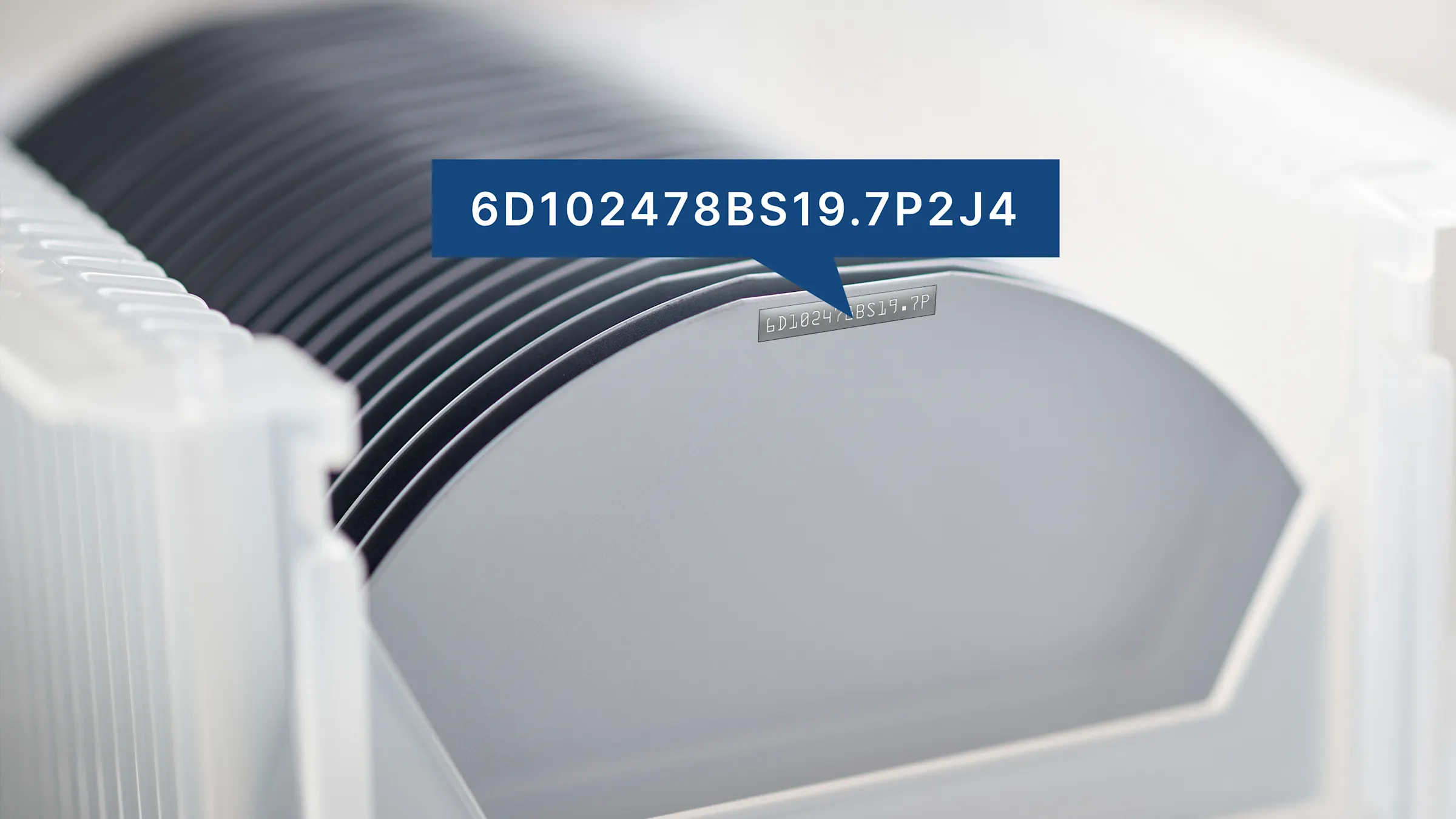
Wafer edge OCR involves reading small alphanumeric characters laser-marked on the outer edge of a silicon wafer. These unique IDs typically follow industry standards such as SEMI M12 or T7 and are essential for traceability throughout the manufacturing process.
Reticles, or photomasks, contain the circuit pattern for each chip layer. A laser-etched ID on the glass or chrome border ensures proper usage and traceability during lithography.
Challenges
Low contrast on reflective surfaces Laser-etched IDs on silicon wafers or chrome reticles often lack contrast, especially on polished surfaces. This makes characters difficult to detect, often leads to missed or incorrect reads. Typically optimized lighting and image enhancement required.
Glare and specular reflection Reflective wafer edges and reticle glass can produce intense glare under standard illumination. Specialized lighting techniques like coaxial or polarizing illumination are essential to reduce saturation and reveal ID details.
Curved or confined marking areas Characters marked on rounded edges may appear distorted or go out of focus. Standard lenses struggle to handle this, especially at high speeds. IDs are often placed on the wafer’s beveled edge or in small areas on photomasks. These zones distort focus and shape, requiring high-resolution imaging and precise optical alignment.
Basler’s integrated vision solution for semiconductor ID reading
Basler offers a configurable vision solution for semiconductor ID reading, designed for easy integration into inspection, dicing, and handling systems. It combines four critical components—high-performance cameras, optimized optics, adaptable lighting, and intelligent software tools—that work together to deliver flexible, reliable performance for wafer edge OCR, carrier ring codes, and substrate IDs. This integrated approach ensures consistent results across a wide range of materials, lighting conditions, and process environments.
How can you improve ID reading on difficult semiconductor surfaces?
See how lighting, optics, imaging, and software can be configured for low-contrast, reflective, curved, or degraded markings.Complete the form to continue reading.