Achieving Reliable Wafer Prober Alignment with Vision
In advanced wafer testing, prober alignment is one of the most demanding vision tasks. With pad pitches below 25 µm and over 150,000 contact points per wafer, alignment relies on detecting fiducial marks on both the wafer and probe card to maintain a unified coordinate system. Basler’s stable imaging, optical precision, and intelligent algorithms help system makers achieve fast, accurate, and repeatable alignment even under deformation or die shift.
Why is alignment critical?
As the semiconductor industry moves into advanced packaging and multi-die architectures, wafer probing plays a key role in ensuring known-good-die (KGD) quality. Each touchdown must achieve micron-level precision because, in 2.5D and 3D packaging (2.5D/3D packaging: advanced chip integration with high demands on wafer alignment), even a slight misalignment can cause poor contact or pad damage, significantly increasing downstream cost.
Unlike probe tip QA, which can be performed offline, alignment occurs during every test touchdown. The system must execute micron-level coordinate correction across the wafer, using multiple fiducial marks and coordinate transformations to compensate for wafer warpage and thermal drift. This makes alignment one of the most challenging vision tasks in wafer testing.
Tackling alignment challenges with vision technology

Sub-micron accuracy with limited optics
At pitches below 25 µm, optical physics inherently limits alignment precision. This includes pixel sampling rate, optical aberrations, depth-of-field constraints, reflection, noise, and contrast. Conventional pixel sizes cannot directly detect sub-micron displacements, while lens aberrations and field curvature amplify errors across large fields of view.
Basler cameras achieve measurement-grade precision through:
High-resolution sensors
Telecentric optics that eliminate perspective errors
Sub-pixel algorithms that interpolate to a fraction of a pixel
Consistency between cameras is critical. Basler ensures:
Strict batch-to-batch quality control
Uniform color response, sensitivity, and noise performance
Minimal recalibration in multi-camera setups

Illumination under reflective surfaces
Copper pads and nickel/gold bumps create mirror-like reflections that saturate sensors, while ultra-thin wafers become semi-transparent, causing interference patterns. Traditional brightfield illumination often fails under these conditions.
Coaxial illumination penetrates surface films while minimizing metallic glare. Dark-field techniques make smooth metals appear dark while preserving alignment mark visibility. Polarized setups eliminate specular reflections. HDR (High Dynamic Range) cameras capture detail in both bright metallic and dark substrate areas simultaneously, while anti-blooming architectures prevent bright reflections from contaminating adjacent pixels.

Fiducial recognition in noisy conditions
Fiducial marks on production wafers are often obscured by CMP residues, particles, scratches, and complex patterning. These artifacts can mask or mimic true fiducials and cause template matching to fail.
Robust recognition requires noise filtering that preserves sharp edges, multi-scale template matching for varying contrast, and adaptive thresholding to correct uneven illumination. Tools such as Shape Centroid Finder further improve localization by calculating the geometric center of fiducial patterns for precise alignment.
These algorithms can run efficiently on the host PC using pylon vTools, or be accelerated in real time within the camera or frame grabber using VisualApplets or Basler frame grabbers, offering flexible architectural choices.
Looking to optimize your alignment workflow? Discuss with us
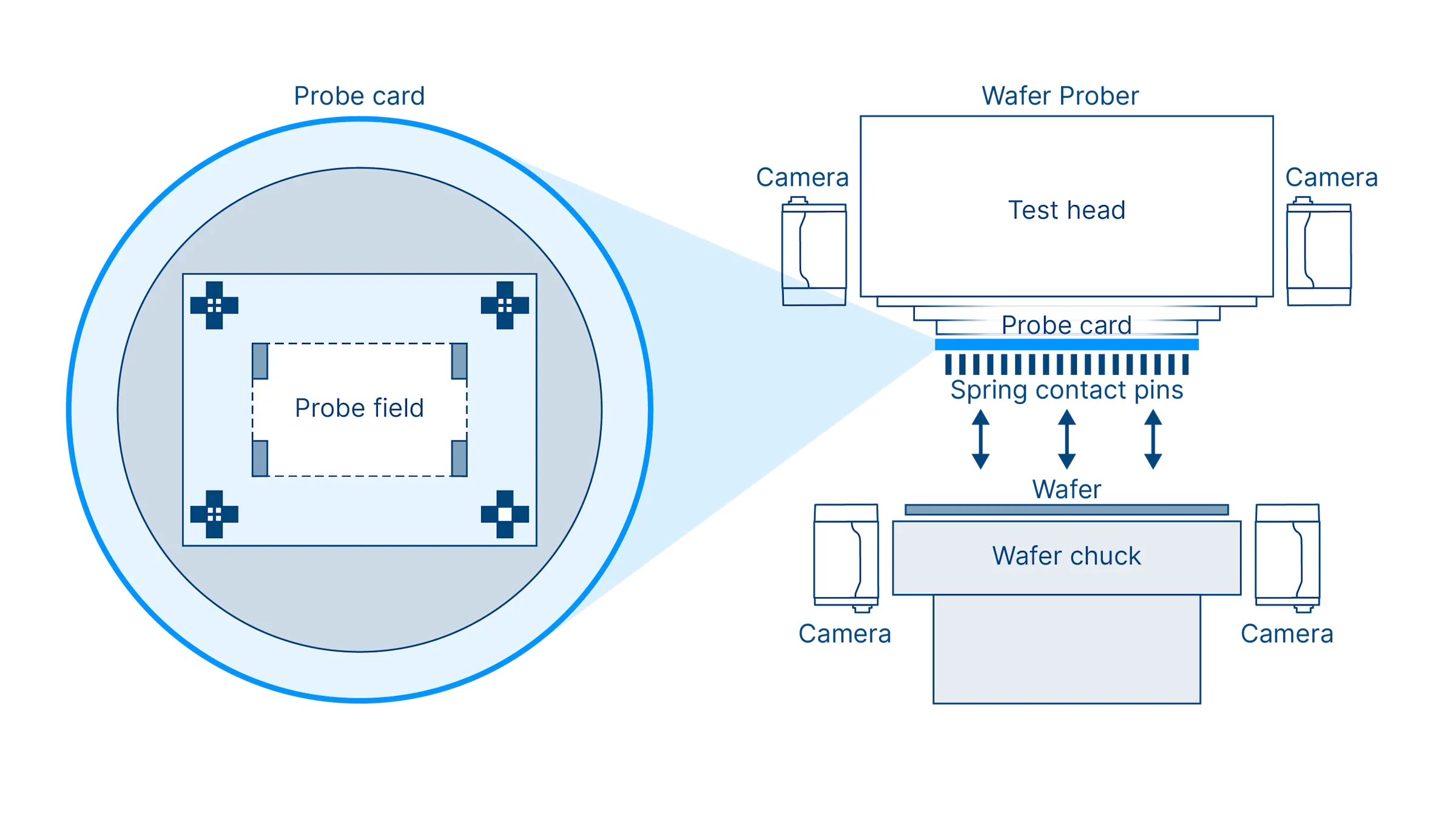
Dual-fiducial coordination for precise alignment
In a prober, the vision system recognizes not only global wafer fiducials but also fixed reference marks on the probe card formed during photolithographic fabrication.
By correlating both fiducial sets, the system establishes a unified coordinate frame that compensates for thermal drift, assembly tolerances, and mechanical offsets, achieving fully automated, high-precision alignment. This dual-fiducial correlation is fundamental to stable probe touchdown and repeatable testing.
Vision techniques correct thermal drift and die shift
During testing, wafers and probe cards are exposed to temperatures from −40 °C to +150 °C, creating thermal expansion mismatches that shift bump positions by several microns. After singulation, dies mounted on film frames may also shift unpredictably, so their actual bump locations no longer match the nominal probe card layout. From a vision engineer’s perspective, both problems are solved with the same toolkit: fiducial recognition through template matching, followed by affine transformation to calculate translation, rotation, and scale corrections. The resulting affine correction matrix is passed to the stage controller, ensuring that probes consistently land on the right pads despite drift or die movement.

Imaging stability and processing efficiency
In advanced probers, alignment accuracy depends not only on resolution and illumination but also on the geometric stability and processing efficiency of the entire imaging chain. Even slight distortion or latency can translate into micron-level errors. Basler ensures synchronized and reliable pre-processing like imaging by integrating hardware-level distortion correction and real-time algorithm acceleration directly in the camera or frame grabber. This reduces host load and increases system throughput, enabling integrators to maintain speed, precision, and repeatability in high-throughput testing.
Alignment may look simple on paper, but in real production, it’s one of the toughest vision tasks to keep stable. Our cameras are deployed in countless alignment systems, from wafer probers to bonding stages, where consistency and reliability are key. What makes Basler stand out is how well our cameras hold precision over time, batch after batch, 24/7.

Achieve repeatable wafer alignment through vision
The result is a vision solution tailored to the demands of advanced prober alignment: not just high resolution, but robust fiducial recognition, real-time affine correction, and stable imaging that ensure probes consistently land on target pads under all thermal and mechanical conditions.
Have wafer prober alignment challenges? Talk to our vision expert.Flexible vision solutions for KGD assurance
By combining optimized illumination, robust fiducial recognition, affine correction, and real-time algorithm acceleration, Basler’s vision solutions ensure stable and repeatable imaging, providing the foundation for achieving the low-defect levels required for known-good-die in advanced multi-die packaging.
Key benefits of partnering with Basler:
Proven in alignment applications: Reliable camera performance across wafer probing and bonding ensures lasting accuracy.
Integration-ready: Optical consulting, distortion correction, and FPGA options simplify system design.
Consistent by design: Exceptional batch-to-batch image stability supports 24/7 operation with minimal recalibration.
This complete imaging-chain design enables fast integration and consistent performance across production environments.
Products for this solution
Looking to implement a comparable solution? These products will help you.


