Use Case

High-speed 2 µm Redistribution Layer (RDL) Inspection

Overcoming vision challenges in advanced packaging

With the rising cost of Known Good Dies (KGD), defect detection and false positive control in Redistribution Layer (RDL) inspection have become critical in the back-end process. As copper RDL linewidths shrink to 2 µm and below, multi-material layer stacking induces substrate warpage, significantly increasing inspection complexity. This directly impacts yield, cost control, and time-to-market. This case study presents a cost-effective, high-speed, line-scan vision solution for RDL inspection.
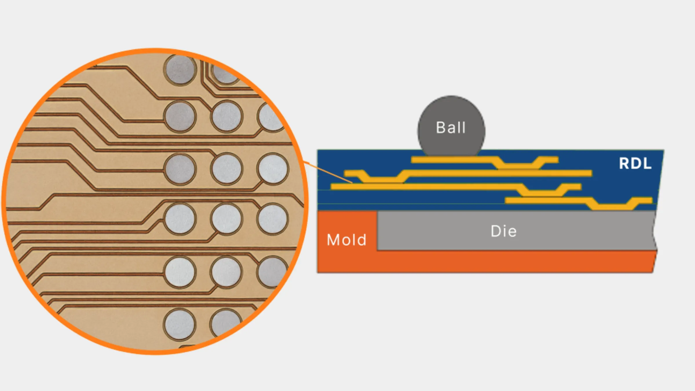
High-Speed Vision Solution for 2 µm RDL Inspection

Application requirements for modern RDL inspection

High-density RDL is a core interconnect technology in advanced packaging, widely deployed in FOWLP, FOPLP, 2.5D and 3D silicon or glass interposers, as well as HBM and chiplet packages. These applications impose unprecedented demands on dimensional accuracy and reliability. Current mainstream RDL technology has advanced to 2/2 µm or smaller dimensions, with 4–5 copper layers now common in fan-out packaging, and even more in leading-edge processes.

Multi-layer structures add inspection complexity, with challenges such as substrate warpage, copper grain noise, and the large data volumes generated by high-resolution scanning. These factors demand precise, consistent imaging for every RDL layer.

Tackling key vision challenges in RDL inspection
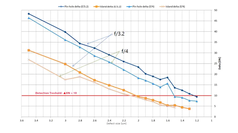

Line scan magnification lens detection capability comparison graph
Detection capability comparison for a line-scan magnification lens: At an f/3.2 aperture, black dot defects (pinholes) are detectable down to 1.2 µm, and white dot defects down to 2.0 µm.

Resolving ≤2 µm features at production speed

Nyquist sampling requires about 0.87 µm/pixel resolution to clearly separate adjacent copper lines in 2/2 µm RDL patterns. While this provides ideal image quality, the high magnification reduces field of view and increases scan time.

A more practical alternative is single-pixel detection, where the smallest critical feature is covered by a single pixel, and detection is based on the pixel’s grayscale delta (ΔDN). For example, with 3.5 µm * 3.5 µm pixels and 1.75× magnification, the object-side resolution is 2.0 µm/pixel, allowing direct inspection of 2 µm RDL features. By quantifying the relationship between feature size and grayscale difference, and setting an appropriate detection threshold, defects can be sperated from background.

As shown in the line graph, at f/3.2 aperture, black dot defects (pinholes) can be detected down to 1.2 µm, and white dot defects (islands) down to 2.0 µm.

Looking to improve your RDL inspection? Talk to our expert.


High Cu graininess from the plating process is the main reason for false positive defects

Suppressing copper grain noise interference

Electroplated copper’s polycrystalline structure is easily mistaken for defects at high magnification. In this case, a beam-splitter coaxial brightfield combined with controlled darkfield illumination is used. This coaxial lighting is integrated with the lens to ensure stable and uniform line illumination. At the image pre-processing stage, morphological and frequency-domain filtering suppresses low-to-mid-frequency texture while preserving high-frequency edge details.

When the noise floor is ≤3 DN, uniformity variation ≤2 DN, and copper grain texture contrast ≤8 DN, combining this with a ΔDN = 10 detection threshold and targeted algorithms enables stable detection of 2 µm island and 1.2 µm pinhole defects. For severe grain or semi-transparent dielectric layers, polarized coaxial or fluorescence-capable lighting can further enhance detection stability.

Multi-layer RDL in fan-out packaging

Maintaining cross-layer consistency

In multi-layer RDL inspection, differences in optical properties between layers, warpage and deformation-induced alignment errors, and copper grain interference from upper layers can all degrade consistency.

To address these issues, the system maintains stable optical and illumination architecture, using coaxial brightfield and darkfield switching, polarized or multi-wavelength illumination, and precise control of DOF and resolution at the imaging stage. On the algorithm side, feature separation filtering and multi-point nonlinear distortion compensation are applied, along with online pre-processing to maintain a consistent noise floor and contrast across layers.

Need stable, repeatable imaging for every RDL layer? Ask us how.


Same-spec lenses can differ greatly in performance. In 5 µm line pair tests, Lens A shows higher contrast than Lens B, confirmed by the wider amplitude range of its profile (blue) compared to Lens B (red).

Balancing high-speed inspection and exposure compensation

FOWLP and FOPLP inspection requires detecting 2 µm defects among a large number of features while controlling false calls, and maintaining high throughput. TDI technology can improve SNR through multi-line integration without reducing scan speed, which is why it is common in these applications.

However, integration requires ultra-high data bandwidth, wide-field optics and illumination, precise synchronization, and stable mechanics; otherwise, performance is limited. System-level evaluation is essential to determine when to enable TDI and how to integrate it to balance optical performance, takt time, and data processing capacity for best results.

Hardware-accelerated real-time pre-processing for wafer inspection

Hardware-accelerated real-time pre-processing

High-speed inspection generates massive data streams, making it essential to move key pre-processing steps into hardware to reduce the host CPU load. Frame grabbers with integrated FPGA processing can perform noise filtering, contrast enhancement, and morphological operations before data reaches the CPU. For copper grain suppression, hardware filters can smooth texture while preserving edge detail, ensuring stability and consistency during high-speed inspection.

While preprocessing improves the detection stability in 2D, another limitation arises when substrates warp beyond the available depth of field. This requires a different strategy.

Illustration of wafer warpage evolution in fan-out packaging, showing the increase from RDL1 to RDL4 due to coefficient of thermal expansion (CTE) mismatch between copper redistribution layers and the mold compound.

Managing warpage in multi-layer RDL substrates

When three or more RDL layers are stacked, peak-to-valley (PV) warpage typically exceeds 40 µm, which is beyond the effective inspection depth of field for the lens setup described in this use case. At this stage, 2D optical adjustments are no longer sufficient. The proper approach is to use 3D inspection methods, most commonly laser triangulation, which capture height maps with micron-level precision.

By combining 2D high-speed inspection with targeted 3D triangulation, fine-pitch 2 µm detection is maintained while warpage beyond the DOF limit is reliably handled.

Our customers face many trade-offs in 2 µm RDL inspection — resolution vs. speed, defect sensitivity vs. false calls, DOF vs. warpage, and data volume vs. inline requirements. We help shorten their trial-and-error process by reviewing AOI system constraints, production targets, and sample data, then providing practical tests and recommendations on lens NA, illumination, and preprocessing. This consultative approach enables faster, more confident integration of the right vision setup.
Park, Benjamin
Park, Benjamin
Head of Optical Solution | Basler APAC R&D

Performance gains for AOI system makers

Our engineering support ensures the right design choices for complex RDL inspection tasks. By combining optical, illumination, and processing expertise, this solution enables AOI makers to meet 2 µm inspection requirements with speed and reliability.

  • Stable ≤2 µm defect detection at production speed, even with copper grain noise and warpage.

  • Optimized BF/DF coaxial lighting and FPGA preprocessing for high edge detection stability and low false positives.

  • System-level approach to balance resolution, takt time, and processing bandwidth.

Looking to improve your RDL inspection? Talk to our expert.


Products for this solution

Looking to implement a comparable solution? These products will help you.

Ready to get started together?

Learn more about our products, services, and how we can help you with your next project.