High-speed BGA Inspection in Semiconductor and PCB Packaging
Unique image pre-processing operators guarantee precision
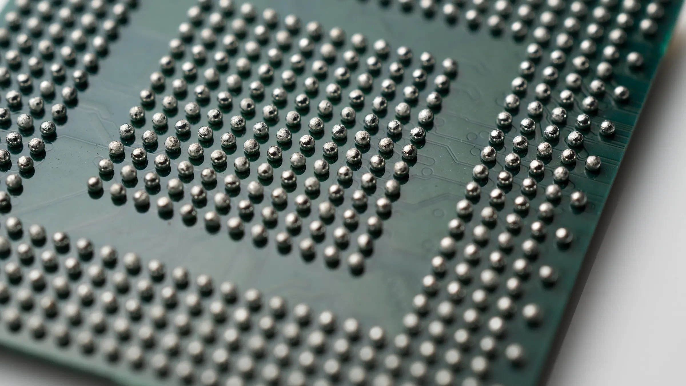
Ball Grid Array (BGA) technology is widely used in semiconductor packaging and PCB assembly, enabling high I/O density in a compact footprint. Before packaging, BGA inspection focuses on verifying the quality of the solder balls themselves, ensuring they are complete, round, uniform in size, and precisely aligned within the array. After reflow, inspection shifts to verifying solder joint quality and placement accuracy, confirming that each BGA is correctly positioned and securely bonded to the PCB.
BGA inspection across semiconductor and PCB packaging
With the advancement of integrated circuit technology, packaging evolved from early DIP (Dual In-line Packaging) to QFP (Quad Flat Packaging) and QFN (Quad Flat No-lead Packaging). As chips became more complex and I/O requirements continued to increase, BGA packaging (with its bottom ball grid structure) has become the mainstream solution and is widely used in consumer electronics, such as smartphones, tablets, motherboards, and digital cameras. Compared with traditional packages, BGA can accommodate more connection points within the same footprint while providing shorter electrical paths, thereby improving signal integrity and overall performance.

In semiconductor packaging, BGA solder balls are mounted onto the substrate as the final step before shipment. Inspection must ensure there are no missing balls, diameter variations, or coplanarity deviations; otherwise, PCB assembly yield may be compromised. In PCB assembly (SMT), BGAs are mounted to the board and reflowed, and the inspection focus shifts to the hidden joints underneath the package. Defects such as voids, head-in-pillow, and opens can all lead to potential field failures.
BGA package sizes range from compact 5 × 5 mm devices to large 50 × 50 mm FC-BGA substrates with thousands of balls. Inspection must be performed with precision from several hundred microns down to tens of microns.
Four key vision aspects in BGA inspection
Comprehensive BGA inspection requires a combination of techniques. On the 2D level, AOI is used to verify whether ball pitch is uniform, the matrix aligns with the design grid, and the array is complete without missing or extra balls. 3D AOI checks solder ball height and coplanarity. In addition, X-ray inspection is required to reveal internal defects, such as voids, head-in-pillow, and opens.
Continue reading: about the four key vision aspects in BGA inspection
Fill in the form to access the complete solution overview.