Machine Vision for Semiconductor Molding Inspection
Semiconductor molding spans conventional packages, advanced packages, wafer-level and panel-level packaging. As molding processes, package structures and workpiece formats change, so do the imaging requirements, from compact in-machine inspection to process monitoring and large-area, high-resolution imaging.
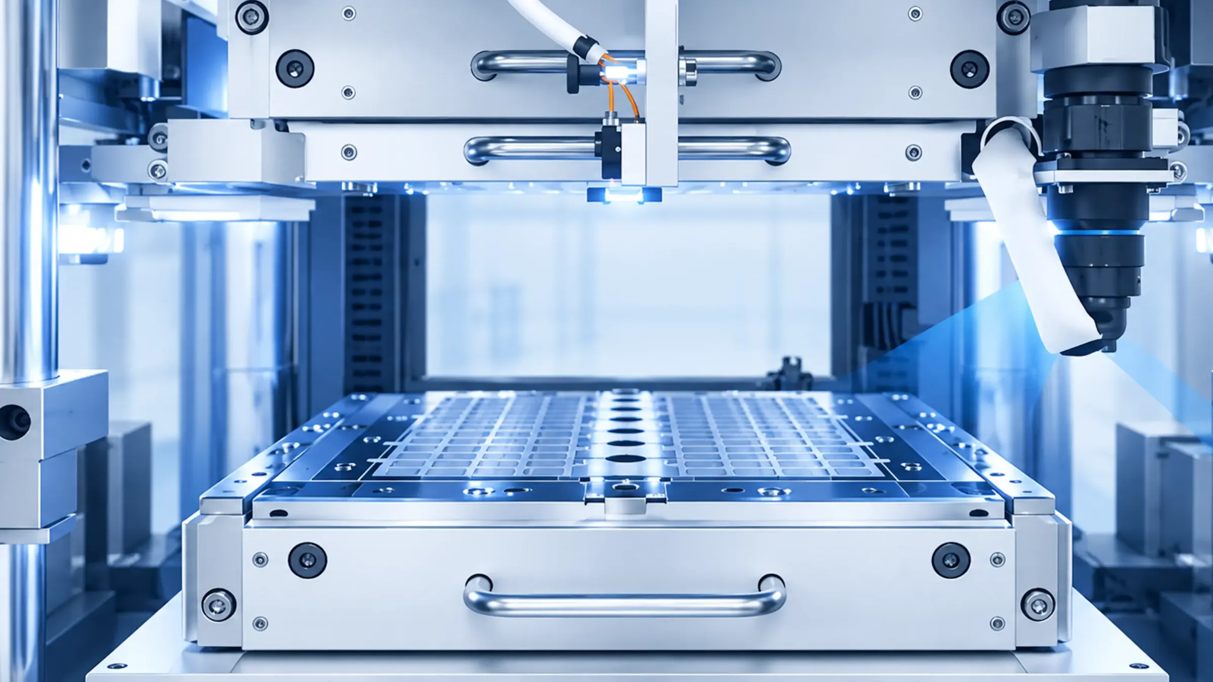
Different molding processes create different vision requirements
Transfer and compression molding can be used across different semiconductor packaging applications. For machine vision, however, the inspection task is also shaped by the package structure, inspection area and process requirements.
Packaging type | Key process characteristics | Imaging requirements |
Conventional packages | Package-level molding and encapsulation, commonly using transfer molding; compression molding is also used for selected package types | Localized inspection depending on the process step, with integration space, FOV and surface contrast as key considerations |
|---|---|---|
Advanced packages | More components and increasingly complex package structures; transfer or compression molding can be used depending on the process | Fine-detail inspection across complex structures and materials, requiring suitable resolution, optics and illumination |
FOWLP | Dies are molded into a reconstituted wafer, typically using compression molding | Die position and post-mold die shift measurement; wafer-scale inspection increases FOV and calibration requirements |
FOPLP | Fan-out packaging extends the reconstituted structure from wafer to larger panel formats, typically using compression molding | Large-area inspection increases the challenge of balancing FOV, resolution, calibration, focus and throughput |
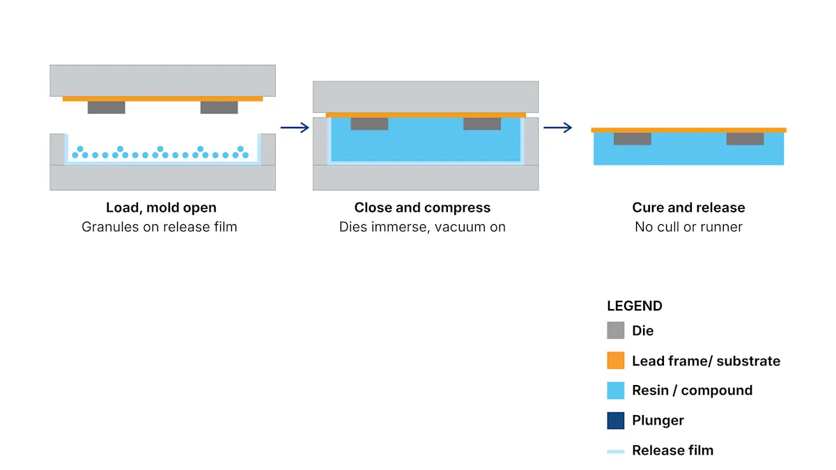
Machine vision inside molding equipment
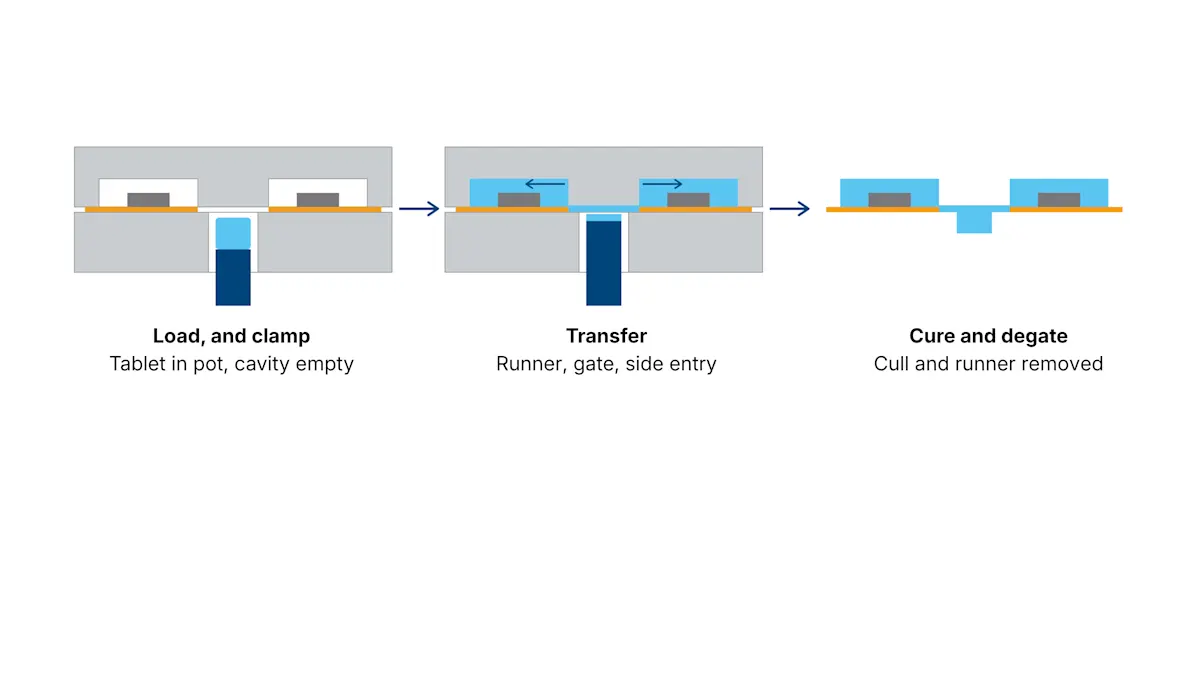
Machine vision can support multiple inspection points before and after molding. While transfer and compression molding have some inspection tasks in common, the imaging requirement can differ due to their resin-handling processes.

Integrating vision within limited machine space
For both molding methods, vision can be used around the molding process for tasks such as workpiece positioning, mold or process-area inspection, and post-mold inspection. The exact inspection point depends on the equipment design and package being processed.
As workpiece and molding areas become larger, using a larger sensor or higher-resolution camera to cover a wider FOV may seem like the straightforward approach. However, a larger FOV can require longer working distances or larger optics, which may not fit within the available machine space. In these cases, compact or distributed camera configurations, such as dart (27 mm × 27 mm) or ace 2 (29 mm × 29 mm) can provide greater integration flexibility while covering the required inspection area.
Discuss your requirement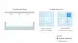
Resin dispense monitoring in compression molding
Compression molding introduces an additional imaging opportunity because the molding material can be dispensed or distributed directly into the mold before compression.
Vision can be used to monitor the resin dispensing area and determine whether the required distribution or pattern is achieved before the molding step. The inspection requirements depend on the resin type, dispensing method and process.
For these applications, the challenge is not only camera resolution. FOV, installation space and sufficient contrast between the resin and mold surface also need to be considered.
Advanced packaging scales the imaging challenge
In fan-out packaging, molding does more than encapsulate individual components. In mold-first FOWLP, dies are placed on a temporary carrier and over-molded to create a reconstituted wafer for subsequent processing. This introduces positional and dimensional challenges that are less prominent in conventional package-level molding.
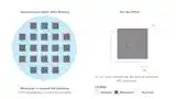
Measuring die shift after molding
During wafer over-molding, dies can move from their intended positions. As downstream interconnect dimensions become finer, knowing the actual die position after molding becomes increasingly important for subsequent processing.
Imaging can therefore move beyond defect detection toward die-position and die-shift measurement, providing coordinate information that can support downstream alignment and process control.

Scaling from wafer to panel inspection
Moving from FOWLP to FOPLP extends similar packaging processes to much larger panel formats. The fundamental challenges—including die shift and warpage—remain, but become more difficult to manage as the processing area increases.
For optical inspection, a larger area must be covered while increasingly fine features still need to remain visible. This creates competing requirements for FOV, resolution and throughput. Panel warpage can further introduce height variation across the inspection area, affecting focus and measurement stability.
As a result, panel-scale imaging systems need to consider not only camera resolution, but also optics, focus strategy, calibration, acquisition architecture and data processing.
Designing your next semiconductor molding system? Discuss with our expertAs semiconductor molding moves from package-level applications toward wafer- and panel-level processes, the imaging challenge changes significantly. Larger inspection areas, die-position requirements and machine integration constraints need to be considered together when defining the camera, optics and illumination.
Imaging considerations for semiconductor molding
The imaging architecture depends on the inspection target, workpiece size, material characteristics and available machine space. Key considerations include:
Application challenge | Imaging consideration |
Limited machine space | Camera size, optics and working distance need to fit within the available installation envelope |
|---|---|
Larger inspection area | Balance FOV and resolution; a single larger camera may not always fit the required optical geometry |
Different material surfaces | Molding compound, silicon and reflective metal can require different illumination and optical conditions to achieve sufficient contrast |
Wafer / panel warpage | Height variation can affect focus and measurement stability across the inspection area |
Higher inspection throughput | Larger FOV and higher resolution increase image data, making acquisition and processing speed increasingly important |
Matching the vision system to the molding application
Semiconductor molding presents different imaging challenges depending on the molding process, package architecture and inspection task. From localized inspection inside molding equipment to wafer- and panel-level inspection, vision systems must balance FOV, resolution, image contrast, integration space and throughput. Camera, optics, illumination and image processing should therefore be selected together according to the application requirements.
Designing your next semiconductor molding system? Discuss with our expertProducts for this solution
Looking to implement a comparable solution? These products will help you.