Machine Vision for Flexible PCB Circuit Pattern and Defect Inspection
Flexible PCB inspection spans very different imaging tasks. Fine circuit patterns require high spatial resolution over large inspection areas, while localized defects such as micro-cracks and fine dimensional metrology require high-resolution imaging over small fields of view. The right imaging architecture helps AOI systems balance defect visibility, inspection coverage, and throughput.
Machine vision across the flexible PCB manufacturing process
Machine vision can be used at multiple stages of FPCB manufacturing, from circuit formation and coverlay processing to final quality inspection. Each stage presents different imaging requirements depending on the material, defect type, inspection area, and required measurement accuracy.
Circuit pattern inspection: Opens, shorts, nicks, residual copper, and deviations in trace width and spacing.
Coverlay and surface inspection: Registration errors, wrinkles, bubbles, delamination, adhesive squeeze-out, contamination, and surface defects.
Mechanical and localized defect inspection: Conductor fractures and micro-cracks in bend zones, stiffener misalignment, edge lift, and substrate deformation.
Dimensional inspection: Outline accuracy, hole position, critical dimensions, and warpage or flatness.
These tasks create very different imaging requirements. One of the most demanding is resolving fine circuit patterns across large inspection areas without compromising production throughput.
Fine patterns challenge both resolution and throughput
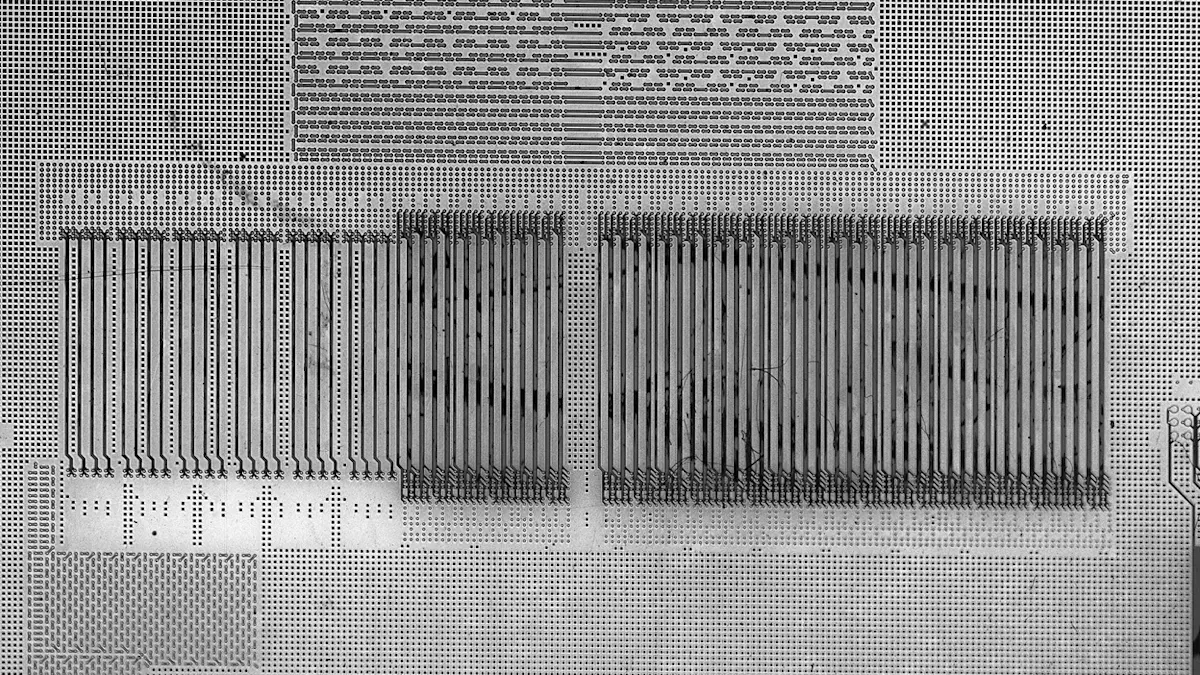
Fine circuit pattern inspection requires AOI systems to distinguish small geometrical deviations and defects such as opens, shorts, necking, residual copper, and irregular trace edges.
Finer features require smaller effective pixel sizes at the object plane. However, increasing optical magnification typically reduces the field of view, meaning more acquisition is required to inspect the same FPCB area.
This challenge becomes more significant when high resolution must be maintained across large panels, sheets, or continuously moving material. As FPCB applications expand into increasingly high-density and high-performance electronics, including AI and HPC systems, AOI equipment must handle growing interconnect complexity while maintaining inspection speed.
Line scan for large-area fine-pattern inspection
For large-area FPCB circuit inspection, line-scan imaging combines continuous acquisition with high spatial resolution. As the FPCB moves beneath the camera, image lines are continuously acquired to build an image of the inspected area.
A higher pixel count across the scan width enables fine spatial sampling over a wider inspection width, making it particularly suitable for inspecting fine circuit patterns across large FPCB areas.
16K line scan for resolution and inspection width
FPCB circuit density has increased significantly: line width and space (L/S) has progressed from around 100/100 µm to 50/50 µm, while advanced flexible-HDI processes now reach 25/25 µm and below. As features become finer, AOI systems require smaller object-side pixel sizes to reliably resolve circuit geometry and defects.
A 16K line-scan camera provides more pixels across the scan width, allowing finer spatial sampling at a given inspection width; or a wider inspection width at a given µm/pixel. This helps maintain inspection coverage as resolution requirements increase, while potentially reducing the number of cameras or scan lanes required.
However, finer sampling also affects the complete imaging system. Optics must provide sufficient resolving power, while smaller effective pixels and shorter exposure times at high line speeds place greater demands on illumination and signal quality. Pixel count, optical resolution, object-side µm/pixel, line rate, illumination, interface bandwidth, and processing capacity therefore need to be considered together.
Talk to our experts about the right imaging architectureParameter
Standard FPCB
Fine-line FPCB
Advanced FPCB (Flexible HDI)
Typical line/space
Typical line/space
~100 / 100 µm
Typical line/space
~50 / 50 µm
Typical line/space
~25 / 25 µm
(and below)
Example image
Example image
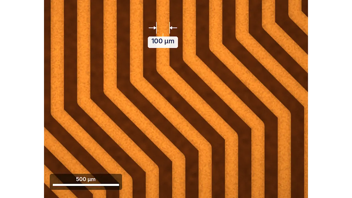
Example image
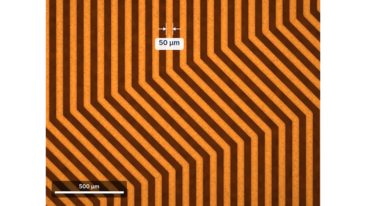
Example image
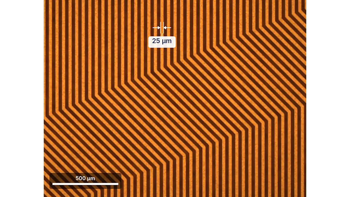
Target object-side sampling
Target object-side sampling
~20–30 µm/pixel
Target object-side sampling
~10–15 µm/pixel
Target object-side sampling
~5–8 µm/pixel
Optics implication (example)
Optics implication (example)
0.17–0.25×
NA 0.05–0.1
Optics implication (example)
0.25–0.5×
NA 0.1–0.2
Optics implication (example)
0.5–1×
NA 0.2–0.4
Illumination implication (example)
Illumination implication (example)
Standard intensity
Illumination implication (example)
2–5× higher intensity
(multi-angle)
Illumination implication (example)
5–10× higher intensity
(multi-angle / multi-strobe)
Camera implication (example)
Camera implication (example)
8K line scan
Camera implication (example)
8K–16K line scan
Camera implication (example)
16K line scan
(possibly TDI)
TDI When the Light Budget Becomes the Limitation
As flexible PCB features move toward 50 µm and below, with advanced processes reaching 25–30 µm, finer object-side sampling is required. Combined with higher inspection speeds, this means shorter exposure times and less signal collected per pixel. At high material speeds, exposure time cannot simply be increased to collect more light without compromising inspection throughput. At the same time, illumination intensity also has practical limits, particularly with low-angle or dark-field illumination, where less light reaches the sensor.
Conventional line-scan cameras can provide the spatial sampling and inspection width required for these applications, but maintaining sufficient signal at high line rates can become increasingly challenging. When the available light becomes the limiting factor, TDI line-scan imaging provides another approach to increasing signal without sacrificing inspection speed.
TDI collects light from the same moving feature across multiple sensor stages, synchronized with the motion of the material. By repeatedly integrating the signal as the feature moves across the sensor, TDI increases the amount of collected signal while maintaining the same material speed. Under photon-limited conditions, the theoretical SNR improvement scales approximately with the square root of the number of TDI stages.
Multiple contrasts in a single material pass
Different flexible PCB defects may require different illumination conditions. Bright-field can emphasize circuit geometry, while low-angle or dark-field illumination can reveal surface irregularities such as scratches, edge defects, or adhesive residues.
With multi-strobe line-scan imaging, different LED groups are triggered sequentially and synchronized with line acquisition. The interleaved lines are then separated by FPGA-based preprocessing into individual image streams. Depending on the system architecture, up to four illumination conditions can be captured in a single material pass, reducing additional scans and processing load on the host system.
As circuit geometries continue to shrink, inspection performance can no longer be defined by pixel count or line rate alone. What matters is how effectively a line-scan camera preserves useful image information throughout the entire acquisition process. Sensor pixel size, optical resolution, and magnification determine how finely circuit features can be sampled, while dynamic range, signal quality, and contrast determine how clearly those features can be distinguished. For high-speed inspection, consistent image quality across the full inspection width and from line to line is equally important. Precise triggering and synchronization with motion and illumination also help maintain consistent image acquisition as the material moves continuously through the inspection system.
High-magnification imaging for localized defects
Localized defects such as conductor fractures, bend-zone cracks, edge damage, and fine dimensional deviations require high optical resolution while maintaining sufficient inspection coverage.
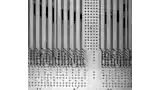
High-resolution area-scan imaging with suitable optics can be used for selected regions of interest or detailed defect review. The achievable resolution depends on the complete optical system, including sensor sampling, lens resolving power, numerical aperture (NA), illumination, and focus, not magnification alone.
As magnification increases, field of view and depth of field (DoF) decrease, making focus more sensitive to FPCB height variation from wrinkles, coverlay, stiffeners, or fixturing. Where this variation exceeds the available DoF, focus control or can help maintain image sharpness at the region of interest.
Evaluate your autofocus requirementsChoosing the right imaging architecture for FPCB AOI
There is no single imaging architecture for all FPCB inspection tasks. The appropriate approach depends on the defect to be detected, required spatial resolution, inspection area, production speed, and available light.
Inspection requirement | Imaging approach |
Fine patterns over large areas | High-resolution / 16K line scan |
|---|---|
High resolution + high speed + limited light | TDI line scan |
Multiple defect contrasts | Multi-strobe line scan |
Localized micro-defects | High-resolution area scan + suitable optics |
Height variation at high magnification | Autofocus |
Designing the camera, optics, lighting, motion, interface, and image processing as one imaging system helps AOI manufacturers achieve the required image quality and throughput without adding unnecessary system complexity.
Products for this solution
Looking to implement a comparable solution? These products will help you.