High-speed 2 µm Redistribution Layer (RDL) Inspection
Overcoming vision challenges in advanced packaging
With the rising cost of Known Good Dies (KGD), defect detection and false positive control in Redistribution Layer (RDL) inspection have become critical in the back-end process. As copper RDL linewidths shrink to 2 µm and below, multi-material layer stacking induces substrate warpage, significantly increasing inspection complexity. This directly impacts yield, cost control, and time-to-market. This case study presents a cost-effective, high-speed, line-scan vision solution for RDL inspection.
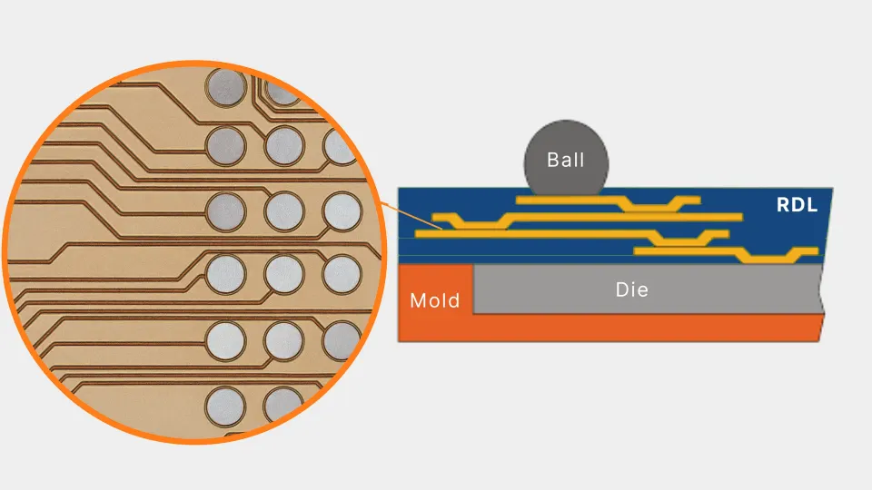
Application requirements for modern RDL inspection
High-density RDL is a core interconnect technology in advanced packaging, widely deployed in FOWLP, FOPLP, 2.5D and 3D silicon or glass interposers, as well as HBM and chiplet packages. These applications impose unprecedented demands on dimensional accuracy and reliability. Current mainstream RDL technology has advanced to 2/2 µm or smaller dimensions, with 4–5 copper layers now common in fan-out packaging, and even more in leading-edge processes.
Multi-layer structures add inspection complexity, with challenges such as substrate warpage, copper grain noise, and the large data volumes generated by high-resolution scanning. These factors demand precise, consistent imaging for every RDL layer.
Tackling key vision challenges in RDL inspection
Resolving ≤2 µm features at production speed
requires about 0.87 µm/pixel resolution to clearly separate adjacent copper lines in 2/2 µm RDL patterns. While this provides ideal image quality, the high magnification reduces field of view and increases scan time.
A more practical alternative is single-pixel detection, where the smallest critical feature is covered by a single pixel, and detection is based on the pixel’s grayscale delta (ΔDN). For example, with 3.5 µm * 3.5 µm pixels and 1.75× magnification, the object-side resolution is 2.0 µm/pixel, allowing direct inspection of 2 µm RDL features. By quantifying the relationship between feature size and grayscale difference, and setting an appropriate detection threshold, defects can be sperated from background.
As shown in the line graph, at f/3.2 aperture, black dot defects (pinholes) can be detected down to 1.2 µm, and white dot defects (islands) down to 2.0 µm.
Looking to improve your RDL inspection? Talk to our expert.
Suppressing copper grain noise interference
Electroplated copper’s polycrystalline structure is easily mistaken for defects at high magnification. In this case, a beam-splitter coaxial brightfield combined with controlled darkfield illumination is used. This coaxial lighting is integrated with the lens to ensure stable and uniform line illumination. At the image pre-processing stage, morphological and frequency-domain filtering suppresses low-to-mid-frequency texture while preserving high-frequency edge details.
When the noise floor is ≤3 DN, uniformity variation ≤2 DN, and copper grain texture contrast ≤8 DN, combining this with a ΔDN = 10 detection threshold and targeted algorithms enables stable detection of 2 µm island and 1.2 µm pinhole defects. For severe grain or semi-transparent dielectric layers, polarized coaxial or fluorescence-capable lighting can further enhance detection stability.
How can you reliably detect 2 µm RDL defects at production speed?
See how to control copper grain noise, maintain cross-layer consistency, manage warpage, and balance resolution with inspection speed.Complete the form to continue reading.