CoWoP Is Coming, and Semiconductor Inspection Is Ready All Along
CoWoP, the emerging system-level packaging innovation, integrates the package substrate and PCB into a single structure, enabling thinner, higher-bandwidth modules with improved thermal performance. To achieve this, the entire PCB supply chain must reach semiconductor-grade accuracy, making advanced vision inspection essential. This article explores how semiconductor inspection technologies can be adapted for CoWoP manufacturing and the key vision inspection challenges shaping its success.

More than a circuit board: CoWoP assigns packaging-level responsibilities to PCB
From CoWoS to CoWoP
The semiconductor and PCB industries are once again redefining their boundaries. As CoWoS (Chip-on-Wafer-on-Substrate) technology matures and powers today’s AI accelerators such as NVIDIA’s H100 and H200, industry attention is shifting to the next major concept — CoWoP (Chip-on-Wafer-on-PCB).
Driven by NVIDIA, with participation from TSMC and major OSATs, CoWoP removes the traditional ABF substrate and directly bonds the silicon interposer to a high-precision PCB, creating a “package-as-system” architecture that merges advanced packaging and large-panel manufacturing.
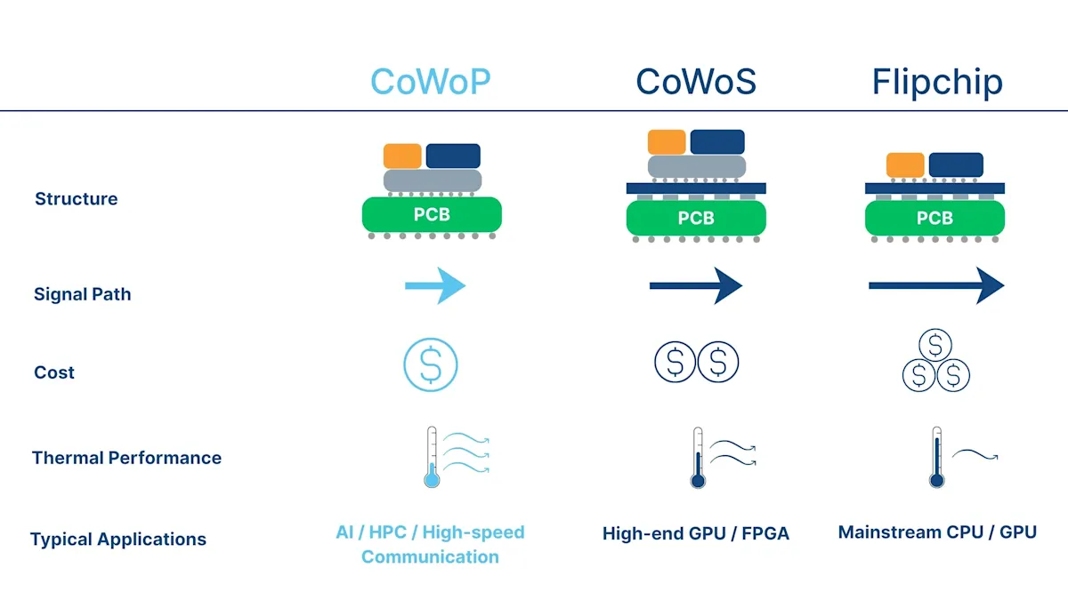
CoWoP advantages
From a technical standpoint, CoWoP offers several clear advantages:
Shorter signal paths improve data latency and power integrity by eliminating the intermediate substrate.
Improved thermal mangement via direct heat-spreader contact.
The removal of ABF/BT substrates and use of large-panel PCB processes can cut packaging costs by 40–50%.
High-throughput PCB panel manufacturing supports faster scaling once inspection and process precision reach substrate levels.
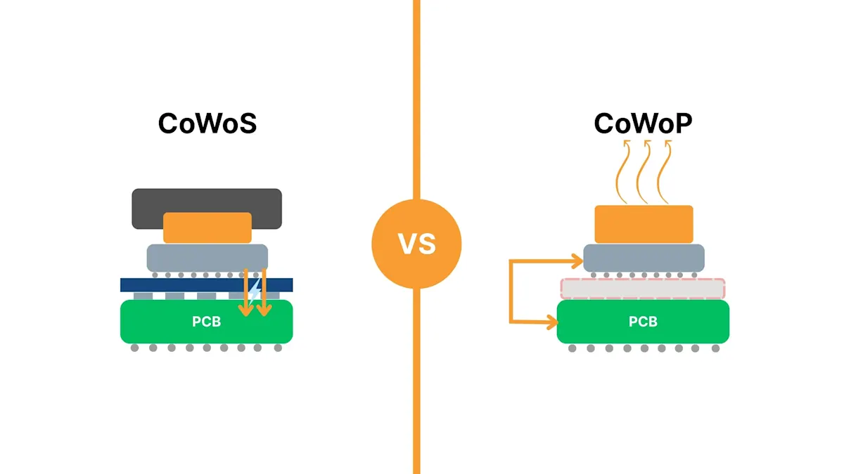

CoWoP demands substrate-like PCB
Yet this transition also elevates the role of the PCB industry.
In the CoWoP architecture, the PCB must not only provide electrical interconnection but also form fine redistribution layers (RDLs) through HDI or mSAP/SAP processes to ensure signal integrity and power delivery.
No longer the passive end of the electronics value chain, the PCB now faces semiconductor-level challenges: building up to 10+ multilayers with 15–20 μm line/space, supporting high bandwidth, low latency, and design flexibility, while maintaining warpage control and material stability comparable to packaging substrates.
If CoWoP needs less precision, why is it harder to inspect?
At first glance, CoWoP’s inspection resolution of 15–20 µm seems less demanding than semiconductor packaging’s < 1–2 µm range. Yet the challenge is greater.

Why easier isn’t easier
First, the inspection area is much larger. CoWoP panel sizes expand to 450 mm × 450 mm, triple the area of a 300 mm wafer.
Second, the material stack is far more complex: a combination of organic substrates (high-performance epoxy), glass-fiber composites, and interleaved metal layers. Uneven reflectivity, variable thickness, and mixed surfaces make high-quality imaging far more difficult.
Third, CoWoP aims to leverage the high throughput of PCB production lines to accelerate output. That means inspection must deliver semiconductor-level precision without becoming the bottleneck in mass production.
So “lower precision” doesn’t make inspection simpler. It makes optical control more multidimensional.
Implication for AOI system providers
For AOI system providers, the significance of CoWoP lies not in chasing higher resolution, but in scaling semiconductor-grade imaging to larger fields of view, faster process feedback, and mixed-material environments.
In this sense, visual inspection often becomes the first indicator of a process’s capability limits. Inspection systems that once operated at the end of the line now need to integrate into the process itself, inline, adaptive, and data-driven.
Traditional PCB vs. Substrate-like PCB
Precision redefined
Compared with traditional HDI boards, substrate-like PCBs used in CoWoP demand a leap in precision, tighter material and warpage control, and more inspection checkpoints throughout the mSAP process. This reshapes how PCB vision inspection ensures yield.
Dimension | Mainstream PCB (standard HDI) | Substrate-like PCB (CoWoP) |
Typical line/space | 50-100 µm | 15-20 µm (and shrinking) |
|---|---|---|
Microvias & pads | ≈ 75–100 µm | Smaller laser vias & pads for 20-30 µm routing |
Interconnect | BGA/CSP with 150–500 µm pitch | Micro-bump with 40–55 µm pitch; Roadmap ≈ 20 µm |
Materials / dielectric | FR-4/standard HDI resins; CTE ≈ 15 ppm/°C | ABF/BT & low-CTE films; CTE ≈ 9–14 ppm/°C |
Warpage | > 100 µm | < 20 µm |
Rework/repair | Mature | Very difficult |
Manufacturing flow | Subtractive etch; Laser-via build-up | mSAP/ABF with fine RDL steps from semiconductor packaging |
Cost | Lower laminate & fab cost | Higher material + process cost; but can offset substrate cost |
What will CoWoP demand from your inspection system?
See the key vision challenges—from fine-pattern inspection to large-panel stability and inline process control—and how semiconductor-proven imaging can address them.Complete the form to continue reading.