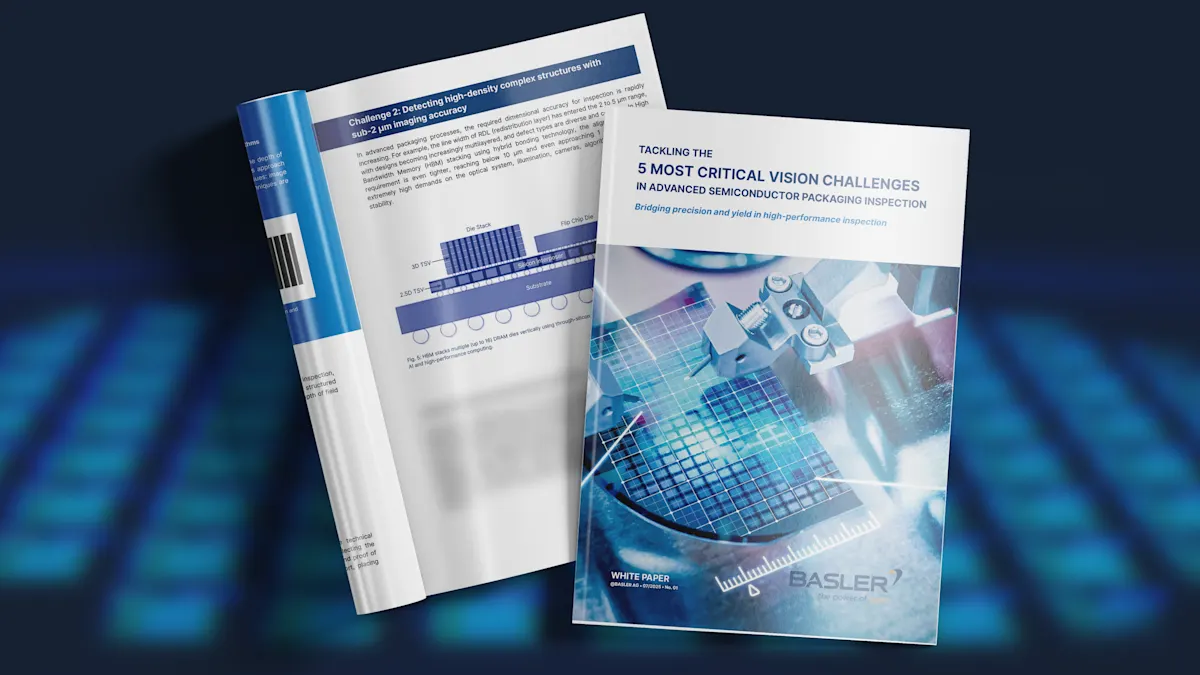
The Top 5 Machine Vision Challenges in Advanced Semiconductor Packaging Inspection
Learn how leading semiconductor OEMs improve yield and inspection accuracy
What’s inside?
This white paper highlights the five key semiconductor inspection challenges today, including:
High magnification lenses that result in shallow depth of field (DoF)
Detecting high-density complex structures with sub-2 μm imaging accuracy
Detecting hidden defects in heterogeneous material systems
The triple demand for real-time performance, high efficiency, and system stability
Growing, yet slow and costly, demand for 3D inspection.
Why does this matter?
Advanced packaging is moving beyond 2.5D/3D integration (CoWoS, X Cube, Foveros) to next-generation semiconductor technologies, such as TGV substrates, FOPLP, and CPO. This shift increases geometric complexity, miniaturization, and new materials like glass cores, driving stricter precision requirements.
Today’s machine vision inspection has evolved from simple quality control to critical inline inspection. However, conventional AOI systems struggle to deliver submicron inspection at the needed production speed.
Who should read this?
OEMs, AOI system integrators, and machine makers developing advanced inspection systems
Vision engineers, system engineers, and R&D leaders driving technology adoption
Purchasing managers and executives evaluating high-precision inspection strategies