Stable Real-Time Wafer Defect Inspection Using High Speed TDI Imaging
In semiconductor front-end manufacturing, wafer surface AOI inspection requires stable detection of submicron defects such as particles, scratches, haze, and contamination for wafer quality and process control applications including CMP, cleaning, and polishing. TDI line scan imaging enables high-throughput acquisition with improved sensitivity under low-light conditions. However, maintaining stable inspection performance also requires synchronization accuracy, calibration stability, and real-time preprocessing throughout the acquisition pipeline.
Maintaining stable acquisition performance in high-speed TDI wafer inspection
As wafer inspection systems move toward higher scan speeds, larger scan widths, and finer defect sensitivity, maintaining stable acquisition performance increasingly depends on synchronization consistency, calibration repeatability, and scalable real-time processing across the full imaging pipeline.
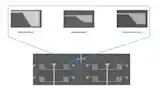
1. Maintaining image integrity during high speed TDI acquisition
TDI image quality depends on the combined stability of optics, geometric alignment, and motion synchronization. Even small deviations can accumulate into irreversible blur during continuous scanning.
At higher magnifications, reduced depth of field increases sensitivity to focus variation and mechanical instability. Real wafers are rarely perfectly flat, and surface tilt or warpage can further introduce focus drift and geometric distortion during high-magnification TDI acquisition.
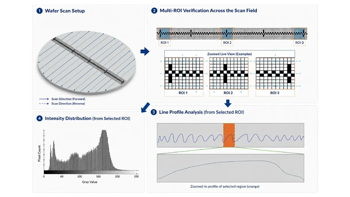
To stabilize image quality, alignment and synchronization must be verified throughout both system setup and continuous scanning.
Structured alignment patterns help verify geometric consistency before enabling TDI accumulation
ROI-based line-profile analysis improves focus and synchronization validation across the field of view
Precise encoder scaling helps maintain image sharpness during continuous motion
Stable synchronization directly affects defect representation quality during high-speed wafer defect detection.
2. Stabilizing calibration across illumination and scan conditions
Different illumination geometries, scan directions, and operating temperatures can introduce shading variation and background instability that affect wafer inspection repeatability.
Maintaining stable calibration across changing operating conditions is therefore critical for consistent defect sensitivity in wafer optical inspection system.
Calibration workflows must adapt to illumination direction, scan orientation, and background variation, since forward and reverse scan directions can introduce different illumination and reflection behavior during continuous wafer inspection.
Illumination-specific FFC sets improve image normalization under varying lighting conditions
Direction-dependent calibration profiles help stabilize bidirectional scanning
Histogram analysis and false-color visualization simplify calibration verification and shading inspection
Stable calibration workflows improve repeatability across illumination and scan conditions in wafer AOI applications.
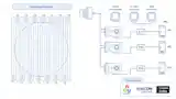
3. Meeting real-time processing constraints at acquisition speed
As scan speed and resolution increase, maintaining stable defect sensitivity becomes increasingly difficult under low-light and high-throughput acquisition conditions.
A 16K TDI camera operating at 500 kHz can generate approximately 8.2 GB/s of raw image data while leaving only microseconds for preprocessing. Even systems using multiple IPCs and GPUs can experience throughput bottlenecks and machine stops between scan sequences during continuous wafer inspection.
Maintaining stable acquisition quality therefore requires preprocessing and reliable high-bandwidth data transfer directly at acquisition speed.
Real-time preprocessing helps stabilize image quality during continuous scanning
Background normalization and adaptive thresholding improve robustness under varying wafer surface conditions
Reliable high-bandwidth data forwarding supports continuous raw-data transfer between frame grabber, GPU, and IPC processing systems
Column-noise suppression helps maintain low-contrast defect visibility
Sustaining stable high-throughput processing becomes just as important as maintaining image integrity in high speed wafer AOI applications.
4. Scaling processing and data handling architecture
Beyond acquisition-time processing, overall system scalability also becomes increasingly important as inspection throughput and scan resolution continue to increase.
Distributing workloads across multiple IPCs and GPU systems can improve scalability, but also increases synchronization and data management complexity.
Distributed IPC/GPU architectures help scale processing capacity for large-area inspection systems
Integrated frame grabber and processing pipelines simplify high-bandwidth data management
Flexible processing architectures support future migration toward FPGA-assisted preprocessing workflows
Scalable processing architecture becomes increasingly important as wafer inspection systems move toward higher scan resolutions and larger data volumes.
Explore our TDI solution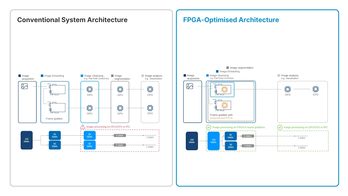
In TDI systems, image quality depends heavily on synchronization and alignment stability. Misalignment introduces irreversible blur in the accumulation direction, while focus inconsistency directly affects defect representation.

At high scan speeds, the challenge is no longer limited to moving data. Maintaining stable acquisition quality while handling synchronization, calibration, and real-time preprocessing simultaneously becomes equally important for reliable inspection performance.

Practical implications for TDI wafer inspection system design
Reliable wafer inspection performance is not defined by sensor capability alone. Maintaining stable high-speed TDI acquisition requires the combined optimization of:
synchronization accuracy
optical alignment and focus
illumination and calibration stability
real-time preprocessing capability
downstream processing architecture
As scan resolution and throughput continue to increase, maintaining image integrity becomes just as important as scaling processing bandwidth and storage infrastructure.
Engineering advantages for high-speed TDI wafer inspection
By combining TDI imaging, real-time preprocessing, and system-level calibration workflows, inspection platforms can achieve higher throughput scalability while maintaining stable acquisition quality under production conditions.
Advantages include:
Stable defect representation during continuous high-speed scanning
Improved synchronization consistency during TDI accumulation
Repeatable calibration workflows across illumination and scan conditions
Reduced downstream processing and storage load
Real-time preprocessing closer to the acquisition source
Scalable architecture for large-area wafer surface inspection
Products for this solution
Looking to implement a comparable solution? These products will help you.
