SWIR Imaging - Applications and Technology
What lies beneath the surface?
SWIR vision systems harness the unique properties of short-wave infrared (SWIR) light to reveal details invisible to the human eye. This advanced technology enables innovative approaches in quality assurance, such as precise material differentiation, temperature detection, and even the ability to see beneath the surface. SWIR imaging often relies on specialized InGaAs sensors for optimal performance in industrial applications.
Multispectral and SWIR technology

In our webinar, we answer the most important questions about SWIR and multispectral imaging:
What is multispectral technology and what is SWIR?
What can they be used for?
What common solutions are there; with what advantages and disadvantages?
Best practice examples
A view toward the future
What is SWIR?
SWIR stands for Short Wave Infrared and refers to the spectral range of electromagnetic radiation between 900 nm and 2,500 nm (nanometers). The human eye, on the other hand, can perceive light from approximately 400 nm to 800 nm.
Material Properties in the SWIR spectrum
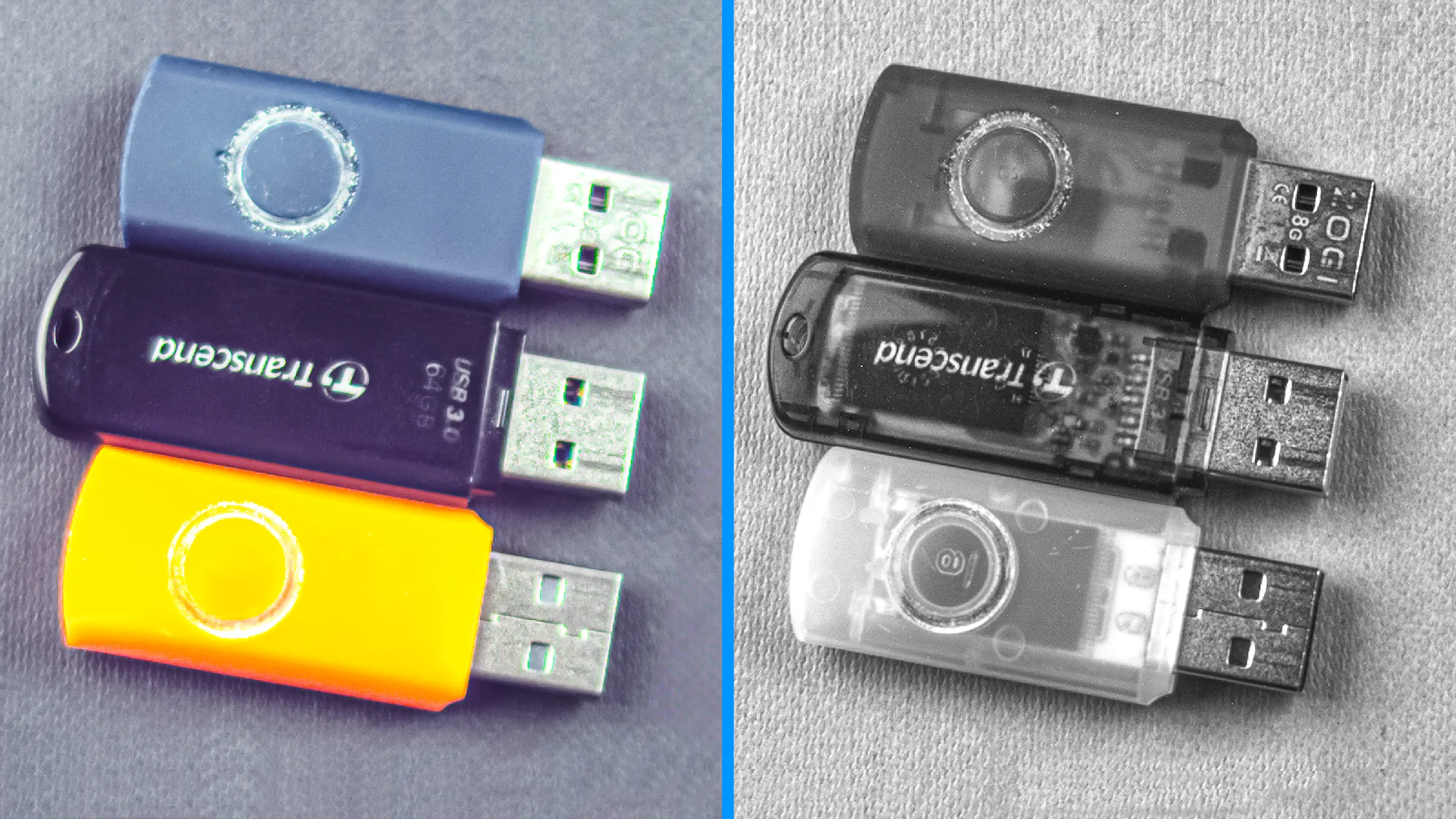
SWIR light has similar properties to visible light: photons interact with objects to create contrast in imaging. Each material reflects, absorbs, or transmits light differently depending on the wavelength.
Silicon, for example, reflects almost all radiation in the visible range; for wavelengths higher than 1,100 nm, it transmits more radiation and thus becomes transparent. Similarly, tinted glass, some plastics, or smoke appear transparent. However, there is also the opposite effect: some materials absorb more radiation in the SWIR spectrum. This results in a higher contrast than could be achieved with shorter wavelengths.
This opens up new possibilities in image processing: salt and sugar, water and isopropanol, or even different types of plastic can be distinguished.
Temperature detection with SWIR imaging
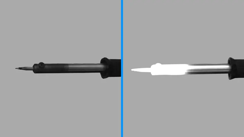
Another application is the detection of heat differences. Objects with a temperature of approximately 140 °C and above increasingly emit infrared radiation, which can be detected with SWIR cameras. The hotter the object, the more infrared radiation it emits, and the brighter the object appears in the image. This means that SWIR technology can offer decisive advantages in process monitoring, as it enables contactless temperature monitoring of materials and products. This is particularly useful in environments where traditional temperature measurement methods are impractical or dangerous.
SWIR vision systems
For image acquisition in the SWIR range, special products are required that are tuned to the short-wave infrared spectrum. Selecting the right components is crucial for the quality of SWIR imaging and requires an understanding of the specific requirements of the respective application.
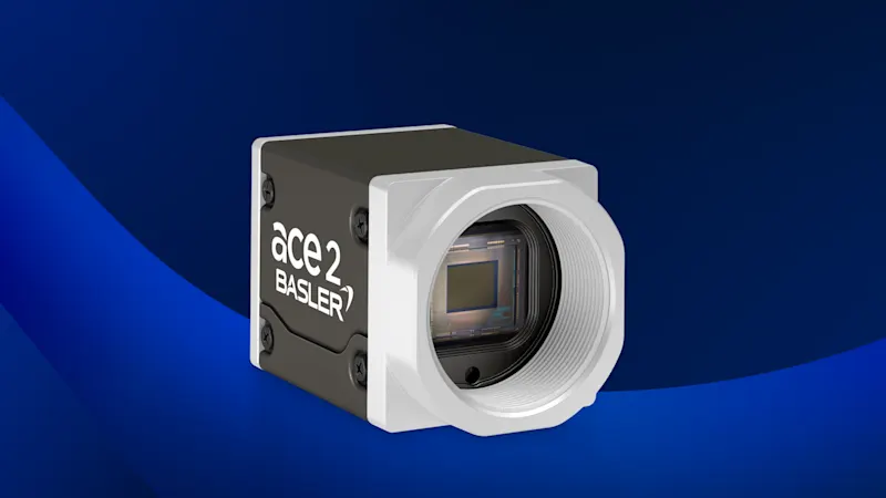
visSWIR cameras
Special sensors are required for SWIR imaging, as conventional silicon sensors have an upper detection limit of around 1,000 nm. Indium gallium arsenide sensors (InGaAs) are particularly well-suited for these purposes as they operate in the typical SWIR spectrum.
visSWIR cameras are sensitive in both the visible and SWIR range. A visSWIR camera can therefore capture both the wavelengths that a camera with a silicon sensor would capture (approx. 400-1,000 nm) and those of the SWIR spectrum. In contrast to previous technologies, which only acquire one or the other wavelength range, these new sensors are suitable for the entire range from 400 nm to 1,700 nm.
SWIR lenses
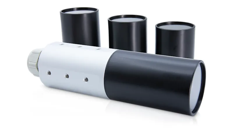
Conventional lenses are usually optimized for the visible spectrum or even filter out the infrared component completely. This is why there are special SWIR lenses that exclude the visible range. In order to provide a sharp image of the entire bandwidth, there are special visSWIR-compatible optics. However, these tend to have a so-called focus shift due to the very large wavelength range. Each wavelength is refracted slightly differently in the optical path of the lens, which is why the focus point moves across the spectral range along the optical axis of the lens. In order to produce a sharp image in the camera, however, the focus point must be as constant as possible. There are special lenses that correct the focus shift. However, if a limited wavelength range is sufficient, cost-optimized lenses without correction are usually sufficient.
SWIR filter
Optical filters play a decisive role for many applications, as they make it possible to control light transmission depending on the wavelength ranges. For visSWIR cameras in particular, it is crucial for some applications to block the ambient light. This increases the contrast at a specific wavelength and highlights individual features.
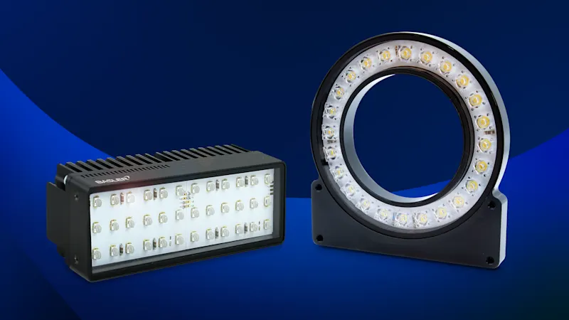
SWIR illumination
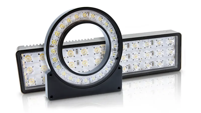
LED lighting indoors generally does not have any wavelengths in the SWIR spectrum. Additional SWIR illumination is therefore necessary, for example halogen lamps with a broadband spectrum or special LED lights that provide a narrowband, defined spectrum. This illumination makes it possible to utilize the sensitivity of the sensor above 1,000 nm.
If a specific wavelength is to be examined, LEDs can be used without additional filters thanks to the narrowband spectrum. This is particularly practical if several wavelengths are to be examined: in this case, different LED spectra can be flashed and a mechanical filter change is no longer necessary. LEDs are more cost-intensive than halogen light sources, but are much more durable and therefore suitable for industrial use. Ultimately, determining which light source is best suited depends on the application.
Applications for SWIR imaging
The following examples illustrate the enormous range of possible applications with SWIR technology across all industries. The use of visSWIR sensors further increases the variety of applications.
Do you need support for your specific application? We would be happy to share our SWIR portfolio tailored to your application in a individual consultation.
What is the technology behind it?
In the past, two cameras or sensor technologies were required to take images in both the visible and SWIR light spectrums. Since then, combined, so-called visSWIR sensors have established themselves on the market. They provide high-resolution images with good image quality.
The SenSWIR technology from Sony
SWIR cameras use either InGaAs (Indium Gallium Arsenide) or CQD (Colloidal Quantum Dot) sensors instead of CMOS sensors. InGaAs sensors were previously limited to quite large pixel sizes and to the SWIR range. Although CQD sensors have smaller pixels and can also be sensitive in the visible range, they offer a significantly lower quantum yield in the SWIR range than InGaAs sensors.
Using Sony's SenSWIR sensors, visSWIR is also possible on an InGaAs basis with a consistently high quantum efficiency over the entire visSWIR range up to 1,700 nm. They are characterized by smaller pixels and thus higher resolutions than conventional InGaAs sensors for very good image quality. This ensures greater accuracy for inspection and quality control in many applications. This is possible thanks to the copper-to-copper connection produced at Sony's semiconductor manufacturing facility. Due to the reduced thickness of the indium phosphate layer (InP layer) compared to conventional SWIR sensors, this sensor is also sensitive in the visible spectrum.
The sensors differ in terms of size and resolution: the first generation IMX990 with 1.3 MP and IMX991 with VGA resolution at a respective pixel size of 5 µm as well as the second generation IMX992 with 5.3 MP and IMX993 with 3.2 MP resolution at a respective pixel size of 3.45 µm. These are used for the Basler ace 2 X visSWIR models.

