ID Reading and Traceability in Semiconductor Manufacturing
Overcome Low Contrast and Surface Variability to Maximize ID Reading Accuracy
Traceability is critical in semiconductor manufacturing. Basler’s solutions enable accurate ID reading—from wafer edge OCR to FOUP barcodes, reticle IDs, substrate codes, and carrier ring markings—ensuring reliable tracking across all stages.
Precision traceability from wafer to final package
Throughout the semiconductor manufacturing process, identification markings must be reliably read to maintain complete traceability. These markings include barcodes, OCR codes, DataMatrix codes, and QR codes that can be laser-etched, dot-peened, or printed on various surfaces with different optical properties.

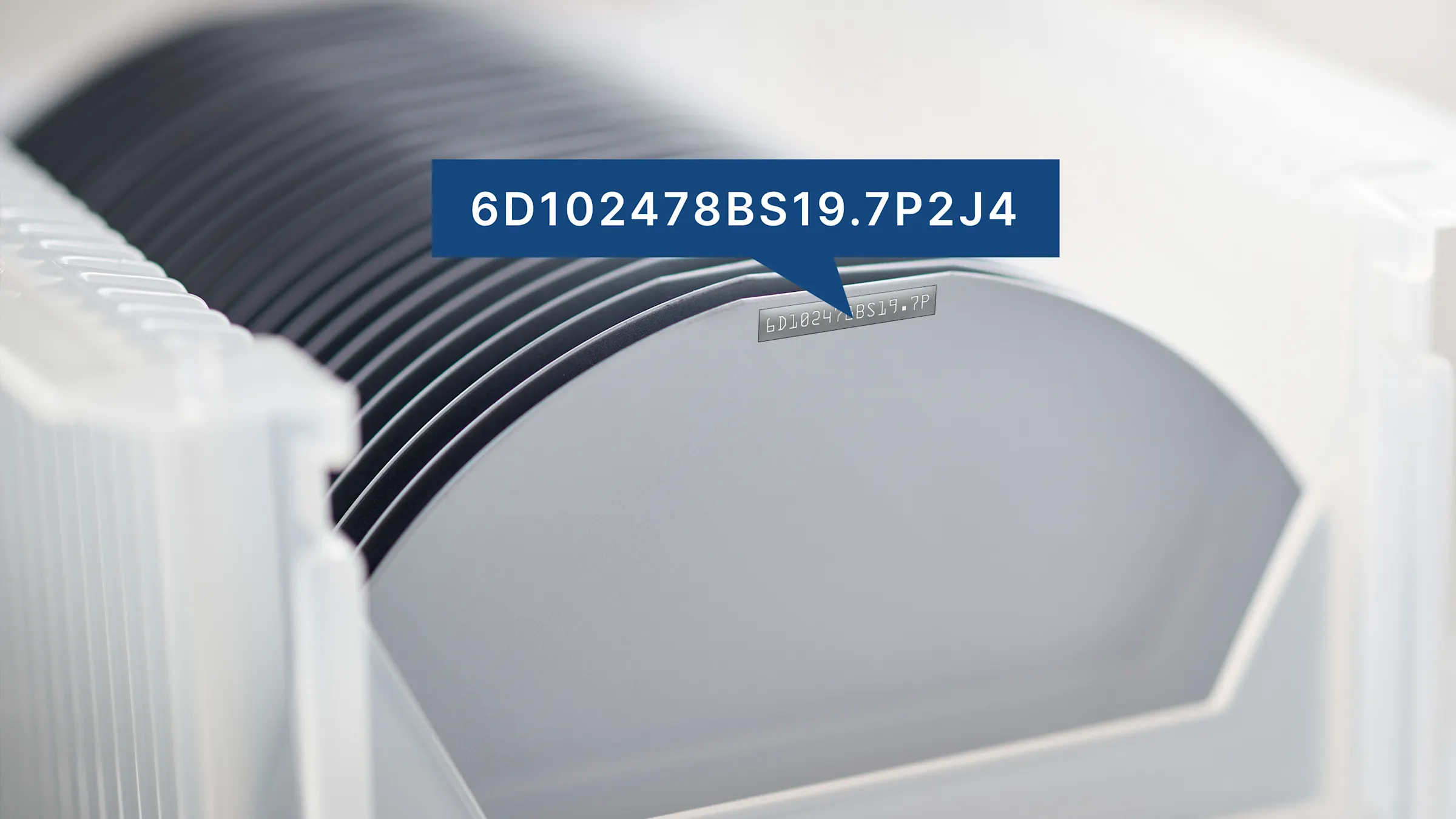
Wafer and reticle ID reading
Wafer edge OCR involves reading small alphanumeric characters laser-marked on the outer edge of a silicon wafer. These unique IDs typically follow industry standards such as SEMI M12 or T7 and are essential for traceability throughout the manufacturing process.
Reticles, or photomasks, contain the circuit pattern for each chip layer. A laser-etched ID on the glass or chrome border ensures proper usage and traceability during lithography.
Challenges
Low contrast on reflective surfaces Laser-etched IDs on silicon wafers or chrome reticles often lack contrast, especially on polished surfaces. This makes characters difficult to detect, often leads to missed or incorrect reads. Typically optimized lighting and image enhancement required.
Glare and specular reflection Reflective wafer edges and reticle glass can produce intense glare under standard illumination. Specialized lighting techniques like coaxial or polarizing illumination are essential to reduce saturation and reveal ID details.
Curved or confined marking areas Characters marked on rounded edges may appear distorted or go out of focus. Standard lenses struggle to handle this, especially at high speeds. IDs are often placed on the wafer’s beveled edge or in small areas on photomasks. These zones distort focus and shape, requiring high-resolution imaging and precise optical alignment.

Carrier ring and chip tray reading
Post-dicing, wafers are transferred to carrier rings or substrates for downstream processes such as die attach, wire bonding, and packaging. These components are marked with process-specific IDs that enable traceability of individual dies or batches during handling and assembly. However, reading these IDs reliably poses unique vision challenges due to material properties, surface wear, and environmental variability common in back-end environments.
Challenges
Surface irregularities & lighting variability: Carrier rings often have curved or uneven surfaces that scatter light unpredictably. Combined with cleanroom lighting variability, this creates shadows or glare, requiring precise, directional illumination for consistent ID reading.
Mark degradation over time: Thermal cycles, chemical exposure, and mechanical wear degrade ID marks, increasing OCR error rates. Robust decoding and image preprocessing are essential.
Low contrast on polycarbonate surfaces: Polycarbonate offers poor visual contrast for etched or engraved IDs, making reliable code detection difficult without enhanced lighting or imaging.
Basler’s integrated vision solution for semiconductor ID reading
Basler offers a configurable vision solution for semiconductor ID reading, designed for easy integration into inspection, dicing, and handling systems. It combines four critical components—high-performance cameras, optimized optics, adaptable lighting, and intelligent software tools—that work together to deliver flexible, reliable performance for wafer edge OCR, carrier ring codes, and substrate IDs. This integrated approach ensures consistent results across a wide range of materials, lighting conditions, and process environments.
Image Acquisition | High-resolution cameras with sensitive sensors capture fine details even in low-contrast or worn markings. High Dynamic Range (HDR) imaging helps handle high reflectivity and uneven lighting, typical of silicon and chrome surfaces. |
|---|---|
Lighting Options | Coaxial (bright field) lighting: Direct illumination, ideal for reading on flat and reflective surfaces like wafer edges or photomasks. Low-angle ring (dark field) lighting: Enhances surface texture visibility, useful for polymer-based carrier rings or textured substrates. Recommend to position at an angle degree from the horizontal plane to highlights surface features. Programmable lighting control: Enables switching between lighting modes to adapt to different materials or mark types on the same inspection line. |
Optics | Telecentric lenses (0.5× or higher): Recommended for small ID marks where distortion and perspective error must be minimized. Standard lenses: Used in scenarios where depth of field or flexible working distances are more important than subpixel accuracy. Autofocus function: Improves read reliability in dynamic environments, especially during in-motion inspection or when handling mixed substrate thicknesses. |
Software | AI-Powered OCR image analysis software: Accurately reads distorted, worn, or curved markings using deep learning. Code Reading image processing software: Supports OCR, DataMatrix, and QR codes across wafers, rings, and substrate. |
Recently, more customers have adopted advanced multi-angle imaging strategies inspired by photometric techniques, yet differences in system design, software integration, and implementation methods continue to create challenges.

Choose flexible, high-performance ID reading solution for semiconductor traceability
Achieving reliable ID reading in actual production environments often requires a flexible, system-level approach. In customer evaluations, we frequently encounter significant variability in environmental conditions and inspection requirements—even when testing the same ID types—resulting in diverse vision system configurations across companies. Basler’s imaging solutions are designed to meet the complex demands of semiconductor identification —ensuring reliable ID reading across diverse materials, surface conditions, and process stages.
Whether you're working with curved wafer edges, low-contrast polymer surfaces, or degraded codes, Basler delivers key benefits:
Reliable reading on surfaces where standard ID readers struggle
Advanced image processing to improve clarity and correct distortions
Deep learning algorithms that adapt to mark wear and variability
Customizable configurations to fit your inspection or system integration
With Basler, system makers and integrators gain a robust, scalable platform for end-to-end traceability—from front-end wafer handling to back-end packaging and beyond.